GY273 QMC5883L Triple Axis Magnetometer Breakout

This is a small breakout, which is different from another already shared here. It has the the same chip, but different footprint and pinout. The silkscreen has the writing HMC5883L, but actually it is a QMC5883L (different I2C registers, etc.)


GY273-QMC5883L.fzpz (5.6 KB)

1 Like

Welcome to Fritzing parts creation hell :slight_smile: , over all not bad, but there are a few problems one of them (gerber generation) fatal.
I have fixed up both parts as new parts (varient2) so you can load both parts at once and made a test sketch in which I will point out the problems.

test_Sketch.fzz (37.6 KB)

The comments below refer to this sketch (which contains both parts). Breadboard is by and large good as is, I chose to redo the scaling to make it match that recommended in the parts format document, but that isnā€™t user visible. I also changed the scale of the part from being width * height in px to width * height in inches, again no visible change but is more usual. The three data pins on both parts are connected to three pin headers and the power to single pin headers (doesnā€™t matter here but does in schematic). If we now switch to schematic, we start to see appearance problems (which donā€™t affect the operation of the part). You will see the wires connecting to your part are ending in the middle of the pin, that is because you donā€™t have the connectorxterminal rectangles defined in the schematic svg (they are in the fzp file). On this part (the GY273) you will see the order of the pins differs between breadboard and schematic, again an appearance issue, not functional. Pcb view in fritzing looks fine, but when you generate gerbers (such as to cut a pcb) things are fatally wrong. This is the gerbv (a gerber viewer) output of the pcb view as a gerber:

The part on the left in each pair is my corrected version, your two from the original parts are scaled incorrectly and donā€™t connect correctly (likely because of translates in the pcb svg although I didnā€™t check). While both new parts will be in the temp bin of the test sketch above, I will upload a copy of the fixed parts to both these parts so people coming along later can just grab the corrected part. If when you look at the svgs of the new part you canā€™t figure out what I did, feel free to ask, the more people making parts the better as far as Iā€™m concerned :slight_smile:

GY273-QMC5883L_fixed.fzpz (7.0 KB)

Peter

Hi Peter, thank you for your review! I will make some investigation, because I donā€™t understand well how to evidence the problem in Fritzing. I use perhaps an old version (0.9.3b on a GNU/Linux Debian stable), and I can load the part nicely, and I can connect with other parts on the breadboard an on the PCB. But I must admit that the original SVGs come from a Python script that I wrote, which generates the SVG from some lines of Python code. I was tired by Inkscape which generates a SGV nightmare, full of warnings and glitches when imported in Fritzing!

As you can see from the screenshot below, in my Fritzing the size error is not visible :frowning:

Unfortunately so far .9.3b is the latest version. Development has stalled ā€¦

Interesting! I still use Inkscape, but I have a python script (available on github) that post processes the output from Inkscape to clean up some of the stuff Fritzing doesnā€™t like and Iā€™m currently working on making it do even more. The base problem is Inkscape is trying to be an svg editor, and Fritzing has limitations (for instance not liking the px on the end of a font-size that the CSS standard calls for.) The best solution I think is to post process the svg output to make it compatible with Fritzing. Iā€™d like to be able to pre compile translates so that we donā€™t have to process them at every render, but I think that is going to be complex. For now Iā€™m looking to automatically remove tspan from the svgs, as that is currently causing problems in Qt (and there are some in parts in core parts) which is currently blocking building Fritzing from source to fix the libgit2 problem on Windows).

Yes, this is an unfortunate fritzing quirk that I have been bit by before :slight_smile: ), so I automatically output gerbers when checking a part and make sure the two agree. The Qt render that renders the pcb view is more capable than the code (which I think is partly an external to the Qt package) that produces the gebers, so in some cases, as here, it looks fine in Fritzing but not when displayed as a gerber. This is undesirable because the PCB production houses create the pcb from the gerber, not from fritzing. The gerber output code has trouble with inheritance for instance and it wonā€™t inherit the stroke width from a higher group as one example I have hit (my python script in lines inherited values in the pcb svg to avoid this issue). I think it also has problems with translates sometimes (or perhaps all the time :slight_smile: ), I tend to like to remove translates from parts both for usability and performance reasons (I expect translates in parts have to slow Fritzing down although I donā€™t have proof yet.)

Peter

Hi Peter! It seems that my parts were misinterpreted by the gerbers creator because I used the SVG viewBox property with a misure unit (mm), where instead it is preferable to use an unitless number (if I understand well).
I fixed my Python script, so now it seems that the breadboard, PCB and gerber view is OK. Please, can you check the new part that I attach here?
The actual breakouts are sold with the holes, no soldered pin headers. So I think that I should mark them as female in the connector tab. Is that right? On the actual PCB I wish to have the copper circles for soldering a pin-header female connectorā€¦

Here it is another part designed by me, this time with the units of measure only in the width and height properties:

GYBMEP_BME-BMP280_Breakout.fzpz (6.0 KB)

That shouldnā€™t be correct (my corrected version uses ā€œinā€ as the width and height units). Dimensionless will leave Fritzing to guess at the dpi setting and it sometimes gets it wrong. Safest is to have the width and height in ā€œinā€ or as you did in ā€œmmā€ as then the dpi is defined and Fritzing wonā€™t guess. I can have a look at the original later, I expect there is a translate in there that the gerber is screwing up.

No, female in the connector def causes the connection to not auto connect in breadboard. It is meant to be used when a set of pins will all connect to the same row on the breaboard (Which would short) as with the 6 pins on the end of an Arduino pro mini. Most of the time pins should be male. That parameter is somewhat misleading as it only applies in breadboard view and isnā€™t about which type of connector it is (although it sounds like it should be :slight_smile: ).

That is easy enough to do, it just needs to be a standard pad with (assuming the desired 1/100 scale in viewbox where 1px = 1 thou in) a stroke-width of 20 and a hole diameter of .078 in. This gives a .038 hole in the pad which fits a .1 header pin.

The check script is fairly unhappy with this :slight_smile: The ones below marked Warning wonā€™t usually break Fritzing but the ones marked Error usually will make the part malfunction.
This starts with the fzpz file unzipped in to a directory which gives these files:

(this happens to be under cygwin on Windows, but it works
fine on linux as long as you have python3 and lxml loaded).

Formatting from the cut and paste is running a bit funny here but it should be understandable. In a bit Iā€™ll have a look and point out what it is complaining about and how to fix it. Unfortunately the error messages assume that you understand the format of the fzp file so they can be less than entirely clear. The first bit details what the script changed in the input svg to fix up Inkscape issues and is mostly for information about what changed (I usually ignore it unless I want to verify the changes). Then come the warnings which wonā€™t usually cause the part to not work but are abnormal, and then the Errors which will cause the part to not work.
The terminalId missing in schematicView (likely an error) warning is indicating you donā€™t have a terminalId in the fzp file which means in schematic the connection will be to the middle of the pin which is usually incorrect (but will work, just look ugly, thus a warning).
$ ls

part.GYBMEP_BME_BMP280_5736cf44ad4cd56ca6e39a45222a2cb2_26.fzp
svg.breadboard.GYBMEP_BMEB_MP280_991354af0812478a25ae9516313ed379_17_breadboard.svg
svg.icon.GYBMEP_BME_BMP280_991354af0812478a25ae9516313ed379_17_icon.svg
svg.pcb.GYBMEP_BME_BMP280_991354af0812478a25ae9516313ed379_17_pcb.svg
svg.schematic.GYBMEP_BME_BMP280_991354af0812478a25ae9516313ed379_17_schematic.svg

$ FritzingCheckPart.py part.GYBMEP_BME-BMP280_5736cf44ad4cd56ca6e39a45222a2cb2_26.fzp
File
ā€˜part.GYBMEP_BME-BMP280_5736cf44ad4cd56ca6e39a45222a2cb2_26.fzp.bakā€™

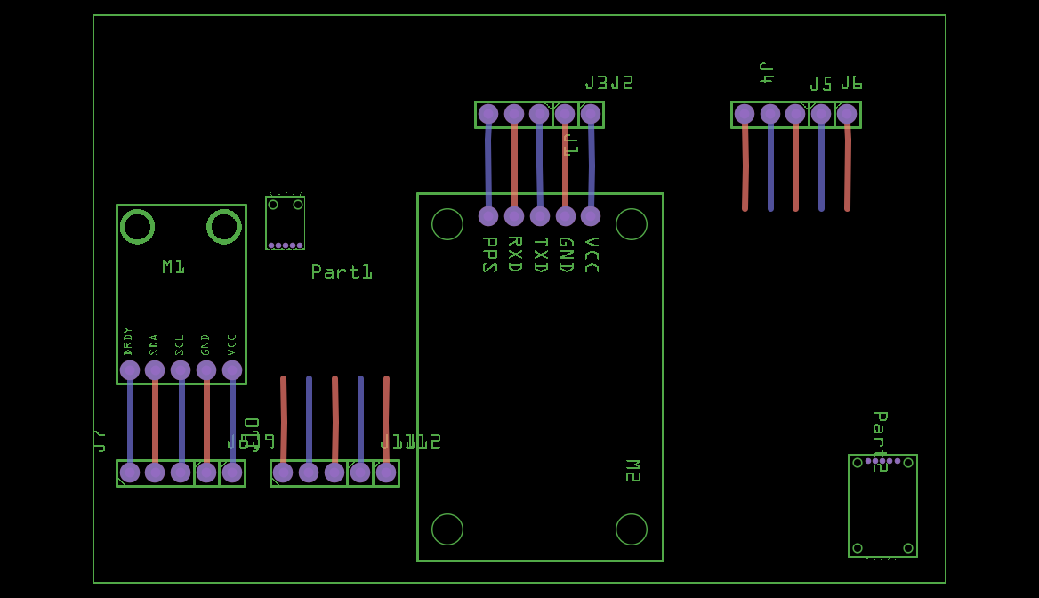
This is a through hole part as both copper0 and copper1 views are present.
If you wanted a smd part remove the copper0 definition from line 39

Modified 4: File
ā€˜svg.breadboard.GYBMEP_BME-BMP280_991354af0812478a25ae9516313ed379_17_breadboard.svg.bakā€™
At line 5

ReferenceFile

ā€˜GYBMEP_BME-BMP280_breadboard.svgā€™

doesnā€™t match input file

ā€˜GYBMEP_BME-BMP280_991354af0812478a25ae9516313ed379_17_breadboard.svgā€™

Corrected

Modified 4: File
ā€˜svg.schematic.GYBMEP_BME-BMP280_991354af0812478a25ae9516313ed379_17_schematic.svg.bakā€™
At line 14

ReferenceFile

ā€˜GY_Schaltplan.svgā€™

doesnā€™t match input file

ā€˜GYBMEP_BME-BMP280_991354af0812478a25ae9516313ed379_17_schematic.svgā€™

Corrected

Modified 4: File
ā€˜svg.pcb.GYBMEP_BME-BMP280_991354af0812478a25ae9516313ed379_17_pcb.svg.bakā€™
At line 5

ReferenceFile

ā€˜GYBMEP_BME-BMP280_pcb.svgā€™

doesnā€™t match input file

ā€˜GYBMEP_BME-BMP280_991354af0812478a25ae9516313ed379_17_pcb.svgā€™

Corrected

Warning 6: File
ā€˜part.GYBMEP_BME-BMP280_5736cf44ad4cd56ca6e39a45222a2cb2_26.fzp.bakā€™
At line 2

ReferenceFile name

ā€˜SparkFun_BME280_Breakout.fzpā€™

Doesnā€™t match fzp filename

ā€˜GYBMEP_BME-BMP280_5736cf44ad4cd56ca6e39a45222a2cb2_26.fzpā€™

Warning 11: File
ā€˜part.GYBMEP_BME-BMP280_5736cf44ad4cd56ca6e39a45222a2cb2_26.fzp.bakā€™
At line 49

Type female is not male (it usually should be)

Warning 14: File
ā€˜part.GYBMEP_BME-BMP280_5736cf44ad4cd56ca6e39a45222a2cb2_26.fzp.bakā€™
At line 56

terminalId missing in schematicView (likely an error)

Warning 14: File
ā€˜part.GYBMEP_BME-BMP280_5736cf44ad4cd56ca6e39a45222a2cb2_26.fzp.bakā€™
At line 71

terminalId missing in schematicView (likely an error)

Warning 14: File
ā€˜part.GYBMEP_BME-BMP280_5736cf44ad4cd56ca6e39a45222a2cb2_26.fzp.bakā€™
At line 86

terminalId missing in schematicView (likely an error)

Warning 14: File
ā€˜part.GYBMEP_BME-BMP280_5736cf44ad4cd56ca6e39a45222a2cb2_26.fzp.bakā€™
At line 101

terminalId missing in schematicView (likely an error)

Warning 23: File
ā€˜svg.schematic.GYBMEP_BME-BMP280_991354af0812478a25ae9516313ed379_17_schematic.svg.bakā€™
At line 144

Key -inkscape-font-specification
value ā€˜DroidSans, Normalā€™ is invalid and has been deleted

Warning 20: File
ā€˜svg.pcb.GYBMEP_BME-BMP280_991354af0812478a25ae9516313ed379_17_pcb.svg.bakā€™
At line 81

copper1 layer should be at the top, not under group copper0

Error 53: File
ā€˜part.GYBMEP_BME-BMP280_5736cf44ad4cd56ca6e39a45222a2cb2_26.fzp.bakā€™
At line 112

Bus nodeMember connector8 doesā€™t exist

Error 53: File
ā€˜part.GYBMEP_BME-BMP280_5736cf44ad4cd56ca6e39a45222a2cb2_26.fzp.bakā€™
At line 113

Bus nodeMember connector11 doesā€™t exist

Error 53: File
ā€˜part.GYBMEP_BME-BMP280_5736cf44ad4cd56ca6e39a45222a2cb2_26.fzp.bakā€™
At line 116

Bus nodeMember connector9 doesā€™t exist

Error 53: File
ā€˜part.GYBMEP_BME-BMP280_5736cf44ad4cd56ca6e39a45222a2cb2_26.fzp.bakā€™
At line 117

Bus nodeMember connector13 doesā€™t exist

Error 53: File
ā€˜part.GYBMEP_BME-BMP280_5736cf44ad4cd56ca6e39a45222a2cb2_26.fzp.bakā€™
At line 120

Bus nodeMember connector7 doesā€™t exist

Error 53: File
ā€˜part.GYBMEP_BME-BMP280_5736cf44ad4cd56ca6e39a45222a2cb2_26.fzp.bakā€™
At line 121

Bus nodeMember connector14 doesā€™t exist

Error 53: File
ā€˜part.GYBMEP_BME-BMP280_5736cf44ad4cd56ca6e39a45222a2cb2_26.fzp.bakā€™
At line 124

Bus nodeMember connector6 doesā€™t exist

Error 53: File
ā€˜part.GYBMEP_BME-BMP280_5736cf44ad4cd56ca6e39a45222a2cb2_26.fzp.bakā€™
At line 125

Bus nodeMember connector15 doesā€™t exist

Error 64: File
ā€˜part.GYBMEP_BME-BMP280_5736cf44ad4cd56ca6e39a45222a2cb2_26.fzp.bakā€™

Connector0 doesnā€™t exist when it must to stay in sequence

Error 69: File
ā€˜svg.breadboard.GYBMEP_BME-BMP280_991354af0812478a25ae9516313ed379_17_breadboard.svg.bakā€™
At line 9

Found a drawing element before a layerId (or no layerId)

Error 77: File
ā€˜svg.schematic.GYBMEP_BME-BMP280_991354af0812478a25ae9516313ed379_17_schematic.svg.bakā€™
At line 26

terminalId connector4terminal canā€™t be a g as it wonā€™t work.

Error 77: File
ā€˜svg.schematic.GYBMEP_BME-BMP280_991354af0812478a25ae9516313ed379_17_schematic.svg.bakā€™
At line 47

terminalId connector3terminal canā€™t be a g as it wonā€™t work.

Error 77: File
ā€˜svg.schematic.GYBMEP_BME-BMP280_991354af0812478a25ae9516313ed379_17_schematic.svg.bakā€™
At line 89

terminalId connector5terminal canā€™t be a g as it wonā€™t work.

Error 77: File
ā€˜svg.schematic.GYBMEP_BME-BMP280_991354af0812478a25ae9516313ed379_17_schematic.svg.bakā€™
At line 110

terminalId connector2terminal canā€™t be a g as it wonā€™t work.

Error 77: File
ā€˜svg.schematic.GYBMEP_BME-BMP280_991354af0812478a25ae9516313ed379_17_schematic.svg.bakā€™
At line 131

terminalId connector1terminal canā€™t be a g as it wonā€™t work.

Error 69: File
ā€˜svg.schematic.GYBMEP_BME-BMP280_991354af0812478a25ae9516313ed379_17_schematic.svg.bakā€™
At line 142

Found a drawing element before a layerId (or no layerId)

Peter

Another fairly long post of the issues :slight_smile:

fpz file:

part.GYBMEP_BME-BMP280_5736cf44ad4cd56ca6e39a45222a2cb2_26.fzp

Connectors should start at 0 not 1 and be in sequence (which they are)

    <schematicView>
      <p svgId="connector2pin" layer="schematic"/>

needs to be replaced with

    <schematicView>
      <p layer="schematic" svgId="connector1pin" terminalId="connector1terminal"/>

to define the terminalIds for all pins in schematic

type should be male (as they arenā€™t in conflict with other pins)

The bus section needs to be removed as it isnā€™t used: In this case as there are no pins in use that are in the bus definition it wonā€™t hurt anything, but neither does it do anything except take up space and processor cycles.

< buses>
< bus id=ā€œsdi/sdaā€>
ā€¦
< /bus>
< /buses>

replaced by

< buses />

(note the two blanks in this need to be removed, without them the forum takes this as formatting commands and doesnā€™t display them) as you donā€™t need any buses.

bb svg svg.breadboard.GYBMEP_BME-BMP280_991354af0812478a25ae9516313ed379_17_breadboard.svg

Scale is incorrect. The desired one (from the parts file format document at

https://github.com/fritzing/fritzing-app/wiki/2.1-Part-file-format

is 1000 dpi:

"For example, many Fritzing files use inches as units, and use 1000 dpi as the basis for the viewBox. So you might see something like

< svg width=ā€˜0.46684inā€™ height=ā€˜0.20306inā€™ viewBox=ā€˜0 0 466.84 203.06ā€™ >"

basiclly the view box should be 100 times the height and width (when the width is in inches (giving 1px = 1 thousandth of an inch).

I correct this in Inkscape by

edit select all

record the coord values in the tool bar

x 0.000 y -0.000 w 39.685 h 52.913

edit->preferences->behavior->transforms->Scale stroke width

ticked (I usually want it unticked)

Then in

File->document properties-> page

Scale x 0.26458

Custom size Units is mm

xml editor first element

height 14.00mm

width 10.50mm

viewBox 0 0 10.50 14.00

Change units to inches and height and width change:

height 0.55118108in

width 0.41338584in

now change the scale to 10.41667

edit->select all (the drawing has more or less disappeared)

x 0.000 y 51.569 w 1.008 h 1.344 px

change that back to

x 0.000 y -0.000 w 39.685 h 52.913

and the drawing will be rescaled to the appropiate scale

height 0.55118108in

width 0.41338584in

viewBox 0 0 413.38596 551.18125

(basically 100h and 100width)

If the lines are too thin, you probaly forgot to enable Scale stroke width

Now on to the svg itself:

line 13 layerId is incorrect

<g
id=ā€œpcbā€

should be

<g
id=ā€œbreadboardā€

as the layerId defined in the fzp file. I prefer to ungroup everything at this point as that removes most of the transforms (not polygons though!) and the many useless groups the file exporter added. Now you can move elements around without
Inkscape using transforms. At the end of it all edit->select all and group and name the resulting group breadboard. I would probably show the terminals as pads with a hole in the center, but as is will work fine.

ids copper0 and copper1 are not needed here only the pcb svg, wonā€™t hurt anything but take up space.

pcb svg svg.pcb.GYBMEP_BME-BMP280_991354af0812478a25ae9516313ed379_17_pcb.svg

Inkscape

edit-> select all

The starting coords arenā€™t 0 but x -0.945 -0.945

meaning some of the drawing is outside the view box and will be truncated on import. So first

File->document properties->Resize page to content

to adjust the view box.

then rescale as above Units in 0 0 41.575 54.803

ungroup everything then rescale it.

untick Scale stroke width

Now select connector1pin

set the stroke width to 20 (it was 19.xxxx)

The rescale has turned the circle in to an ellipse

so in xml editor set both rx and ry to 29 (this doesnā€™t move the center of the pad as changing the diameter in the tool bar does).

This sets the pad to 0.078 in w and h with a 20 stroke width. Drilled hole size is

dia (w or h) - 2 * stroke width = 78 - 40 = .038in,

the correct hole size for a .1 square pin instead of the 0.040551 hole the gerber

Untitled Sketch_drill.txt

file specifies for your original part. Note the text still has transforms even after the ungroup. Normally I delete the translate and then move the text back in to the correct position because as noted I think translates are likely a performance problem. I usually use a stroke-width of 10 for the silkscreen lines but the current 20 will certainly work (now the view box has been adjusted so it wonā€™t truncate). Now you re group copper1/copper0 and silkscreen and you are done. On to schematic file

svg.schematic.GYBMEP_BME-BMP280_991354af0812478a25ae9516313ed379_17_schematic.svg

Needs rescaling. Needss a schematic layerId by edit select all, group and name the group id schematic (to match the layerId in the fzp file). Needs 4 rectangles (I prefer h .01 in w .01 in style fill:none;stroke-width:0) then the id changed to connector1terminal and moved to the end of the pin line
where the connection should terminate. Repeat for the other 3 pins (and preferably renumber them to start at 0!). I prefer to make schematic symbols as small as possible, with the pin line being 10thou in (which is more or less the size used on most other components in core). We really need to create some guide lines for part creation but so far time and interest have been lacking. As a style issue I would probably rotate GND and VCC 90 degrees so all the labels read the same way for neatness. I might try and make the rectangle smaller to allow more parts on a single sheet, but with the internal printing the box pretty much needs to be the size it is. Now having pretty much finished with this part, lets look at the original pcb that is the wrong size. So open

/cygdrive/d/fritzing_backup/imported_parts/u-blox-NEO-6M-GPS_Breakout

vi svg.pcb.NE0-6M-GPS_Breakout_a27f9494c4f434a4b065bc26ebc5fc06_11_pcb.svg

Ah, illumination strikes. I see that you defined the view box in mm rather than dimensionless, yes that is probably incorrect and may well be the cause of your problem. That will likely have gone away when I rescaled the original which is why it didnā€™t bite me. Another check to add to the FritzingCheckPart script (this is usually how I find new features :slight_smile: ).

svg xmlns=ā€œhttp://www.w3.org/2000/svgā€ viewBox=ā€œ0 0 24.00mm 36.00mmā€ height=ā€œ36.00mmā€ width=ā€œ24.00mmā€

because while there are transforms in silkscreen (which may or may not cause problems, I think it was not correctly showing the text in the original) it shouldnā€™t have affected the copper side (which has no transforms).

Peter