For a project, I’m trying to create a custom PCB that would have the rough size of an arduino uno shield but with some material removed to accomodate for some features on the arduino board I’m using.
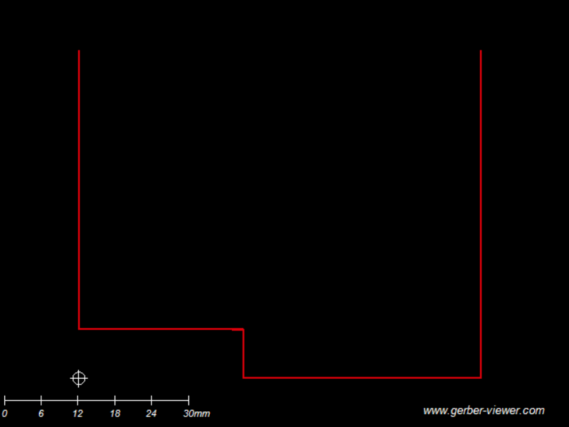
I’m creating my svg in inkscape, but somehow every time I try to export my fritzing project with the custom pcb, the top of the pcb gets lost. Here’s a preview of what my contour.gm1 file looks like in a gerber viewer:
While I am far from an expert in this particular area, it looks like you forgot to resize image to page (at least in Inkscape). Things outside the view box get truncated and that looks to be what is happening here. Loading your pcb-1.svg in to Inkscape and doing edit select all indicates the origin is -0.016 -0.016mm. Try doing (in Inkscape, I don’t know how to do this in the other svg editors):
edit->select all
file->document properties->Page->Custom size->Resize page to content…-> Resize page to drawing or selection
which will change the origin (and more importantly the viewbox) to the size of the document. Save it as plain svg and reimport it and see if that helps. I expect one of our pcb experts will comment if this doesn’t do the trick.
I’m not 100% sure what caused the problem but I do know how to fix it.
First off I did resize the page like Peter suggested because it was 0.2mm smaller than the PCB which would cause an issue similar to what was happening here. But it did not fix it. The problem has to do with the order the path is written in the SVG file and the way I found to get Inkscape to re-write the path was to select the board with the node selection tool and then use “path/simplify” (Ctrl+L)
This fixed the board outline but not the silkscreen. I tried it with your silkscreen layer too but it never shows when I use Aisler to check the results.