OK try this part and see if it does better. There are a variety of problems in your original part. Breadboard is fine, pcb is missing the copper0 layer so thinks it is a surface mount part and will only make connections on the top layer. It also had a translate which I suspect is the source of your clearance problems. Schematic has the most visible changes. I expect you ran it through Parts Editor twice, which has the effect (if you don’t remove the px from font-sizes) of setting the font size to 0 thus the small text in schematic. I also added a label for the part (remove it from the svg if you don’t want it.) This is a new part (I changed the moduleId so it will load along side your original part for comparison.
GSM-Modul-improved.fzpz (6.3 KB)
Some screen shots showing the changes:
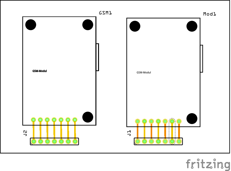
pcb
note in your part on the left all connections are on the top layer because of no copper0 layer in the pcb svg against connections on both layers on the new part on the right. As well in both parts the hole size is 0.035in. Normally for .1 square headers the hole size is 0.038in. If you would like to change that the easy way is edit the pcb svg in a text editor and do a global replace of r=“27.5” with r=“29” which will change the hole size from 0.035 to 0.038in leaving the circle in the same place. As well the mounting holes are in silkscreen. This means that if you make boards, the holes will appear on the silkscreen but not be drilled. This is normal practice for Fritzing (which you may be aware of) and if you want the mounting holes drilled, you drag a hole from the core parts bin in to pcb view and set its size appropriately. It is also possible by changing the pcb svg to always drill the holes (but then someone that doesn’t want the mounting holes drilled needs to change the part to do that, unlike with the hole position in silkscreen.) On to schematic:
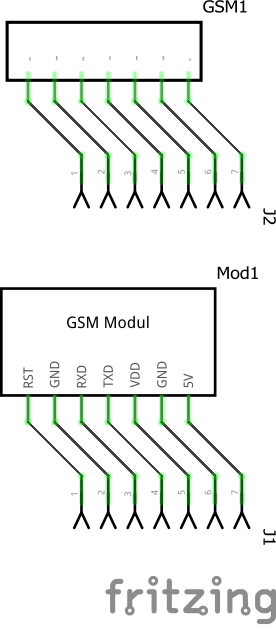
Here your original part is on the top and the labels are too small to read. My part is on the bottom with properly sized labels and a label field telling us what the module is. Hope this helps! If this doesn’t fix you clearance problems you will need to upload the sketch so I can see the problem and try and figure out what is causing it.
Peter
via google translate:
OK, versuchen Sie dieses Teil und sehen Sie, ob es besser tut. Es gibt eine Vielzahl von Problemen in Ihrem Originalteil. Das Steckbrett ist in Ordnung, der Leiterplatte fehlt die Kupferschicht 0, daher wird angenommen, dass es sich um ein oberflächenmontiertes Teil handelt, und es werden nur Verbindungen auf der obersten Schicht hergestellt. Es gab auch eine Übersetzung, von der ich vermute, dass sie die Ursache für Ihre Freigabeprobleme ist. Schema hat die sichtbarsten Änderungen. Ich gehe davon aus, dass Sie den Teile-Editor zweimal durchlaufen haben, was zur Folge hat (wenn Sie die Pixel nicht aus den Schriftgrößen entfernen), dass die Schriftgröße auf 0 gesetzt wird, also der kleine Text im Schaltplan. Ich habe auch eine Beschriftung für das Teil hinzugefügt (entfernen Sie es aus dem SVG, wenn Sie es nicht wollen.) Dies ist ein neues Teil (ich habe die Modul-ID geändert, damit es zum Vergleich neben Ihrem Originalteil geladen wird.
Einige Screenshots mit den Änderungen:
pcb
Beachten Sie in Ihrem Teil auf der linken Seite, dass sich alle Verbindungen auf der obersten Ebene befinden, da in der Leiterplatten-SVG keine Kupfer0-Ebene vorhanden ist, gegenüber Verbindungen auf beiden Ebenen auf dem neuen Teil auf der rechten Seite. Auch in beiden Teilen beträgt die Lochgröße 0,035 Zoll. Normalerweise beträgt die Lochgröße für Überschriften mit 0,1 Quadratmetern 0,038 Zoll. Wenn Sie dies auf einfache Weise ändern möchten, bearbeiten Sie die Datei pcb svg in einem Texteditor und ersetzen Sie r = “27.5” durch r = “29”, wodurch sich die Lochgröße von 0,035 auf 0,038 ändert, wenn Sie den Kreis verlassen am gleichen Ort. Die Befestigungslöcher befinden sich ebenfalls im Siebdruck. Wenn Sie also Bretter herstellen, erscheinen die Löcher auf dem Siebdruck, werden jedoch nicht gebohrt. Dies ist die übliche Vorgehensweise bei Fritzing (die Sie möglicherweise kennen). Wenn Sie die Montagelöcher bohren möchten, ziehen Sie ein Loch aus dem Kernteilefach in die Leiterplattenansicht und stellen Sie dessen Größe entsprechend ein. Es ist auch möglich, durch Ändern der PCB Svg immer die Löcher zu bohren (aber dann muss jemand, der die gebohrten Befestigungslöcher nicht will, das Teil ändern, um dies zu tun, im Gegensatz zu der Lochposition im Siebdruck.) Weiter zum Schaltplan:
Hier befindet sich Ihr Originalteil oben und die Etiketten sind zu klein zum Lesen. Mein Teil ist unten mit richtig großen Beschriftungen und einem Beschriftungsfeld, das uns sagt, was das Modul ist. Hoffe das hilft! Wenn sich das Problem dadurch nicht beheben lässt, müssen Sie die Skizze hochladen, damit ich das Problem sehen und herausfinden kann, was es verursacht.