Assuming this footprint works, this has been a useful exercise in that we should end up with a verified Fritzing friendly microb USB connector which we didn’t have before. Try this one. Note it has a line to indicate where the board edge should be. If positioned correctly at the edge of the board the text on the silkscreen will be truncated as being off board.
Thanks a lot again, Peter!
I think I have the final design then! Time to print and see if everything fits!
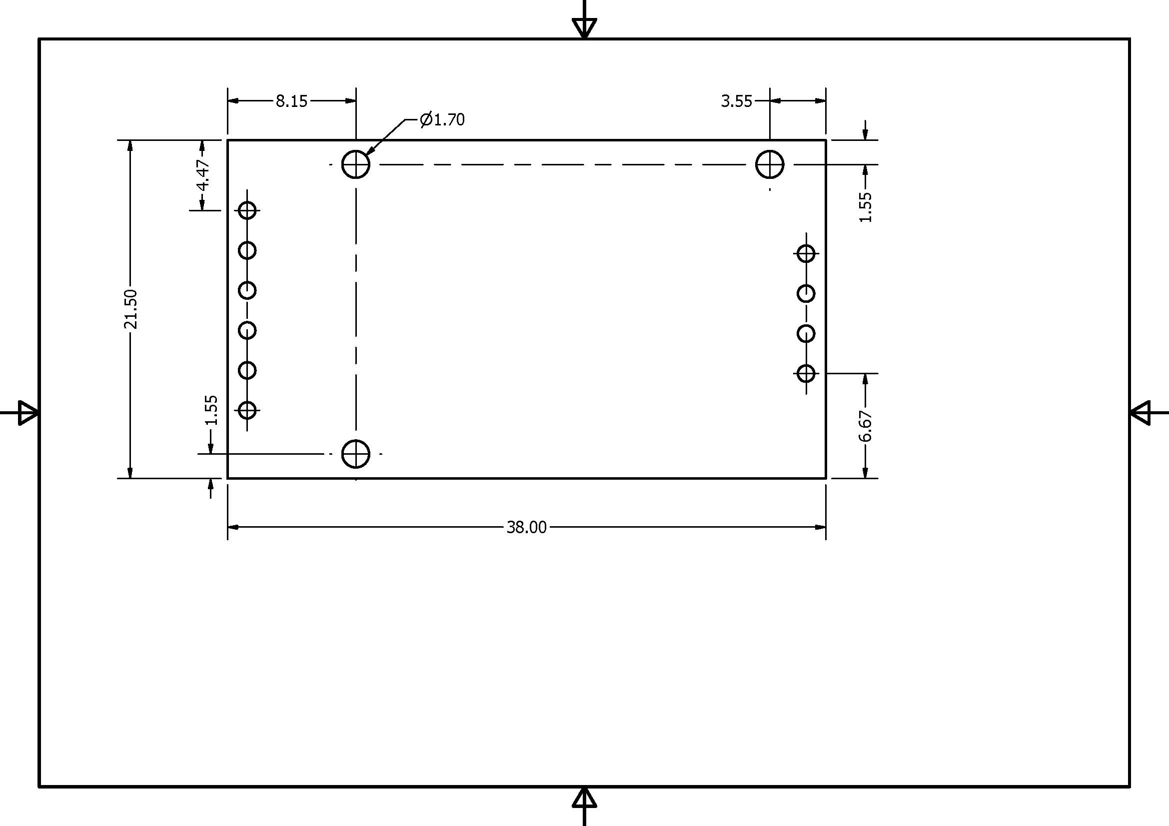
Edit: after checking the etching files, I think the mounting holes for the ZS-042 are not added. Should I add holes for this manually?
Edit 2: I checked the drill file with a Gerber viewer, also the mounting holes for the ZS-042 are there. So I can continue to check PCB with the actual parts.
The mounting holes are showing correctly in both Fritzing and the gerber output for me. I notice if you were really doing USB you probably need a keepout area between the pins and the 4 square pads on the connector to keep the fill out of there but for power it doesn’t matter. Otherwise looks fine.
The usb will be used for usb-purposes; there will be a cable from the usb header pins to the Arduino miniUSB, to feed it with power but also enable me to still program it. Why and how should I design the keepout area for the pads then? In the current drawing the four mounting pads are already separatared, right?
Most USB connectors I have seen (this particular footprint did not) indicate no copper or traces near the USB signal pins presumably for signal integrity reasons (perhaps only on USB3). That may or may not affect you. I don’'t know how you specify a keepout area on fills, perhaps one of our pcb folks will chime in.
I understand what you mean. I double-checked the PCB design rules for USB 3.0 and USB 2.0. The former has quite strict rules about trace width, distance, length matching, etc. USB 2.0 is less fussy about this, the only advice I found is to keep the data traces relatively close and parallel, and not to use over 4" of trace length.
I also noticed that almost all USB 2.0 boards have no copper fill around the signal lines. I removed those from my sketch as well now.
The usb connectors will arrive in a week or so, then I can verify this last but crucial part of the board before ordering. Looking forward to receiving my very first PCB!
This project has been on-hold for some time. Last week I finally had the time to review the PCB. Unfortunately the holes for the ZS-042 RTC module are slightly off.
Any chance I can ask you again to modify the part? The dimensions as I measured them are attached below.
Apart from that, it looked very nice.
Sure I can fix up the part easily enough, but the file doesn’t seem to have uploaded correctly. It looks like it should be a jpg or png file but it won’t save as such and a right click gets me an html file rather than an image file.
OK here is a part modified to move the mounting holes to the new positions in breadboard and pcb. ModuleId is the same as the one above so you will need to remove that one from Fritzing before you can load this one.
If parts editor bites you (a usual occurrence for me ) feel free to post and I’ll edit out the unwanted bits from the underlying files. Its easy to do in the files, I suspect less easy in parts editor.
Thanks for the offer, but I managed!
I simply removed the connections from the Connectors tab in the Parts Editor, and then removed the holes from the pcb’s svg with Inkscape. (For some reason Illustrator completely messed up the drawing.)
Just printed the copper layer and can test the footprints today or tomorrow. One step closer to finishing this project!
Question though about the Parts Editor: I opened the original file first, and saved a copy by ‘Save As’. Now if I edit my custom part again and try to save it, the filename prefix pops up noting that it will also automatically add a unique suffix - though it already has this. On every save, it wants to save a new copy again, cluttering up the library with multiple revisions of the same part.
I’m a bad one to ask about parts editor because I rarely use it. As well it was not finished when development stopped, and is not complete, and I wasn’t involved in Fritzing til after development stopped so don’t know much of what was intended. That said, I suspect the idea is because the prefix is unique and I think probably partially time stamp based, that provides a way to keep generations of a part (much the same as git). I usually find parts editor annoying and edit the underlying files.
So I verified all the PCB footprints, everything looks nice except for one little detail.
The MK5P usb connector has quite narrow soldering pads, that fit nicely with 16 mil traces. For the VCC I drew the standard 24 mil trace, since this supplies the entire board.
Because the trace connects in the centre of the pad, it is very close to the adjacent trace and requires extra low tolerance (and increased costs) for manufacturing.
Other PCBs I saw position the VCC trace off-center to respect the pin spacing. How can I move the trace off-centre?
Sketch added for review. Watchwinder_shield_20190910.fzz (108.3 KB)
I don’t think you can directly. AFAIK the connection is to the center of the pad (and due to a bug, on large traces you need to check the geber output because the bug miscalculates the offsets and sometimes leaves the trace unconnected). The only thing I know that should work is to route the trace from the side like this (I didn’t modify the fills in this):
To do this I set the grid size to .01 in (view->Set Grid size) and it looks like you may still need to move the USB part vcc pad higher a bit to get the center of the pad (where the connection is being made) a bit higher to clear the mounting hole (DRC is complaining about the mounting hole clearance I think). Someone who does more boards than I do may also have an alternate suggestion or trick that I don’t know as well.
That might just do the trick indeed. I already tried something similar with going perpendicular horizontal first, but then the rounded end of the trace was too close still to the adjacent pad.
My other idea was to simply widen the connection pad to the right. But since the mounting hole is in the way there, it would have to be an inverse ‘L’-shape. Not sure if Fritzing allows for that, I’m going to give it a try!
Lo and behold, it worked! In the SVG I simply increased the pad width to the right, then draw a rectangle in the corner that should be removed. With Path > Difference it cut clear the hole again.
Fritzing had no problems with it and place the trace in the centre of the pad.
I exported the PDF and all looked fine. Also verified the Gerber in a Gerber viewer and it works like a charm. The 24-mil trace is now nicely out of the way, which will make manufacturing a lot easier and cheaper
 Time to print and see if everything fits!
 (Do not want the 6-pin connector on my breadboard).