how can ı draw svg for pcb view please help
Your best bet is to copy an existing svg which has the correct groups (silkscreen, copper1, copper0 for through hole, silkscreen, copper1 for SMD.) The tutorials listed in the reply to your part should also help. If they aren’t clear please post your specific question and one of us will answer.
edit: A late thought: are your pcbs done in Eagle? If so there is a program called Eagle2Fritzing which will convert the Eagle brd file in to a Fritzing part. Eagle2Fritzing is a little difficult to build and use (it requires a build environment to build) but is usually easier than doing parts by hand.
Peter
1 Like
no ı use inkspace for desing svg for thıs parts please  add or send pcb svgDENEYAP MİNİ.fzpz (29.2 KB) DENEYAP KART KAMERA.fzpz (37.1 KB) DENEYAP KART.fzpz (23.4 KB)
OK here is a corrected copy of your DENEYAP MINI part posted before. Here are the steps I went through to create this part (this will be long!)
Assumed the comments in the fzp are correct (as they are in turkish!) Connectors are totally screwed so delete them and replace them with boilerplace. Use the pin labels from the part in breadboard to renumber the connectors in the correct order.
31 pins in total, so create boilerplate connectors for 31 pins. Copy the current fzp file to a new one with a new name.
$ cp 'part.deneyap mini_d984197b31308f74e8b59be4cd120401_6.fzp' 'part.deneyap-mini_1.fzp'
edit the new fzp file part.deneyap-mini_1.fzp
and make the following changes.
<?xml version='1.0' encoding='UTF-8' standalone='no'?>
<module fritzingVersion="0.9.6" moduleId="deneyap-mini_1" referenceFile="deneyap-mini_1.fzp">
<version>1</version>
<date>Çar May 26 2021</date>
<label>M</label>
<author>3T VAKFI SEVER (modified by vanepp May 2021)</author>
Change the fritzing version to 0.9.6 (which is what I am using), the moduleId to “deneyap-mini_1” and the reference file to match the current file name “deneyap-mini_1.fzp” . Change the version to 1 (as this is the first version of this part) change the label to “M” to indicate this is a Module (as opposed to an IC or other type of part) add the fact I modified this to the author field. I assume the description and tags are correct (as I don’t read Turkish) and left them alone. Change the family name (which must be unigue!) to something other than ESP32 and set the variant to 1 as this is the first variant.
<property name="family">deneyapmini</property>
<property name="variant">variant 1</property>
change the image file names to the new names for the new part, replace the icon svg with the breadboard svg (saves some space and is what normally happens anyway)
<breadboardView>
  <layers image="breadboard/deneyap-mini_1_breadboard.svg">
    <layer layerId="breadboard"/>
  </layers>
</breadboardView>
<schematicView>
  <layers image="schematic/deneyap-mini_1_schematic.svg">
    <layer layerId="schematic"/>
  </layers>
</schematicView>
<pcbView>
  <layers image="pcb/deneyap-mini_1_pcb.svg">
    <layer layerId="copper1"/>
    <layer layerId="silkscreen"/>
    <layer layerId="copper0"/>
  </layers>
</pcbView>
<iconView>
  <layers image="breadboard/deneyap-mini_1_breadboard.svg">
    <layer layerId="icon"/>
  </layers>
</iconView>
Now delete the connectors section entirely as it is wrong.
  </views>
  <connectors>
  </connectors>
  <buses>
    <bus id="internal1">
      <nodeMember connectorId="connector16"/>
      <nodeMember connectorId="connector13"/>
    </bus>
  </buses>
  <url>https://deneyapkart.org/magaza/urun-deneyap-kart-mini.html</url>
</module>
Now create new a new connector set for 31 pins from
FritzingCreateFzpConnectors.py cons 31
<connectors>
   <connector id="connector0" type="male" name="">
     <description></description>
     <views>
       <breadboardView>
         <p svgId="connector0pin" layer="breadboard"/>
       </breadboardView>
       <schematicView>
         <p svgId="connector0pin" layer="schematic" terminalId="connector0terminal"/>
       </schematicView>
       <pcbView>
         <p svgId="connector0pin" layer="copper0"/>
         <p svgId="connector0pin" layer="copper1"/>
       </pcbView>
     </views>
   </connector>
   <connector id="connector1" type="male" name="">
     <description></description>
     <views>
       <breadboardView>
         <p svgId="connector1pin" layer="breadboard"/>
       </breadboardView>
 ...
       <pcbView>
         <p svgId="connector29pin" layer="copper0"/>
         <p svgId="connector29pin" layer="copper1"/>
       </pcbView>
     </views>
   </connector>
   <connector id="connector30" type="male" name="">
     <description></description>
     <views>
       <breadboardView>
         <p svgId="connector30pin" layer="breadboard"/>
       </breadboardView>
       <schematicView>
         <p svgId="connector30pin" layer="schematic" terminalId="connector30terminal"/>
       </schematicView>
       <pcbView>
         <p svgId="connector30pin" layer="copper0"/>
         <p svgId="connector30pin" layer="copper1"/>
       </pcbView>
     </views>
   </connector>
</connectors>
Note the name and description fields are both blank and need to be filled in from the data in the original fzp file (assuming that is correct.) So load the original part in to Fritzing, and drag it in to a sketch. Select pin 1, the top left pin and hover the mouse over it to bring up the pin label which is A0 41 (indicating it is connector40 in the original fzp file. Now copy the name and description from the original fzp file in to the new one. Repeat for the other pins. Note connector27 D3 shows as RX in the original fzp file, but connector28 is labeled RX as well and there are not likely 2 of them, so RX was deleted from D3. Now we move on the the bus definitions. First we will collect all the ground pins.
GND
12
17
19
3V3
13
18
20
SCL
10
15
SDA
11
16
then create bus definitions for all of them. Finishing the fzp file. Now on to the breadboard svg where we need to renumber the pins to match the .fzp file. Edit the breadboard svg (svg.breadboard.deneyap-mini_1_breadboard.svg) in Inkscape. The first thing of note is the scale is incorrect, so ungroup the entire svg and rescale it to the correct 10.41667 scale like this:
original file
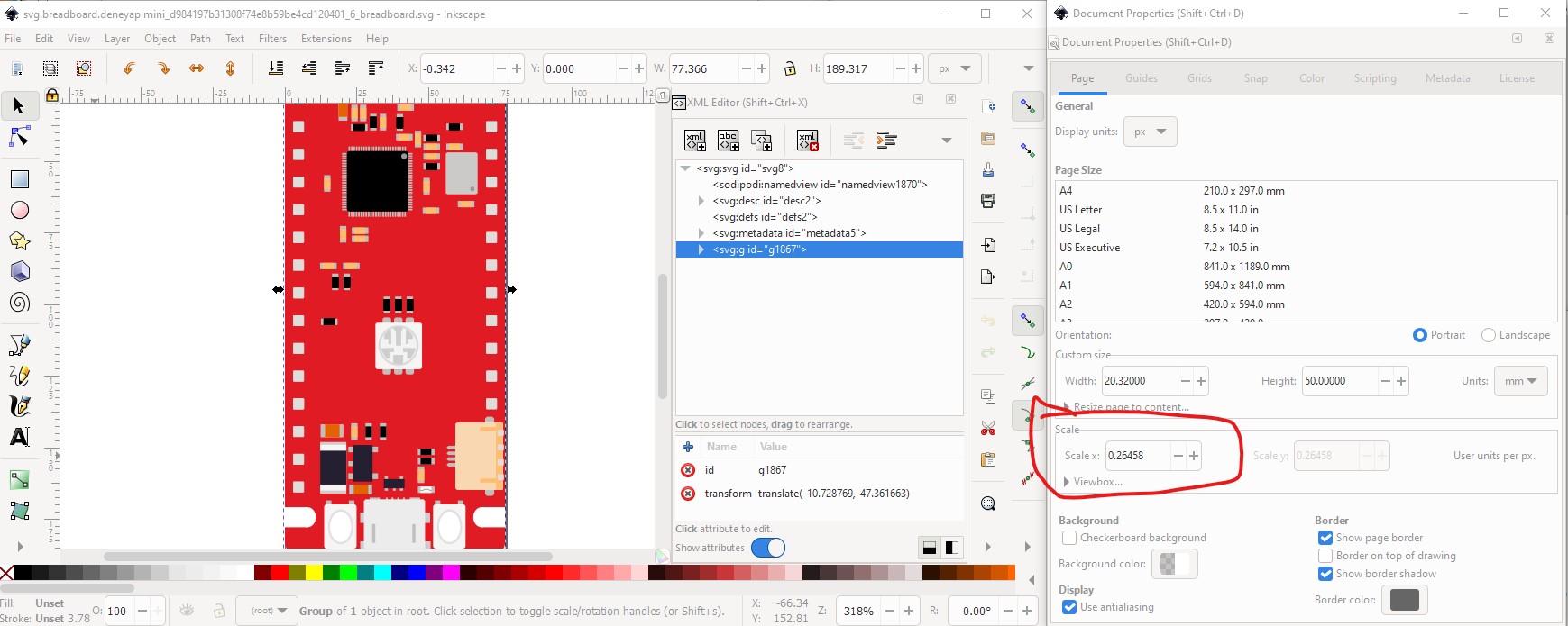
when ungrouped we see that it is not origined at x 0 y 0 which is incorrect,
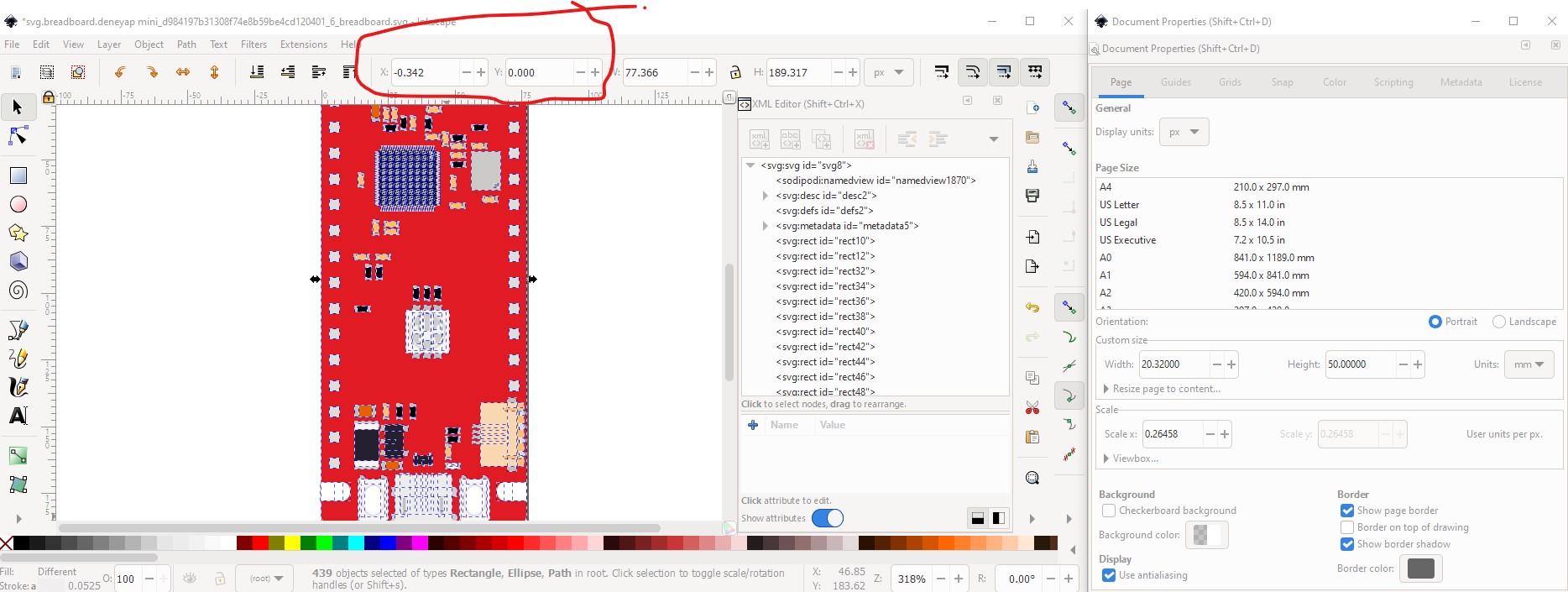
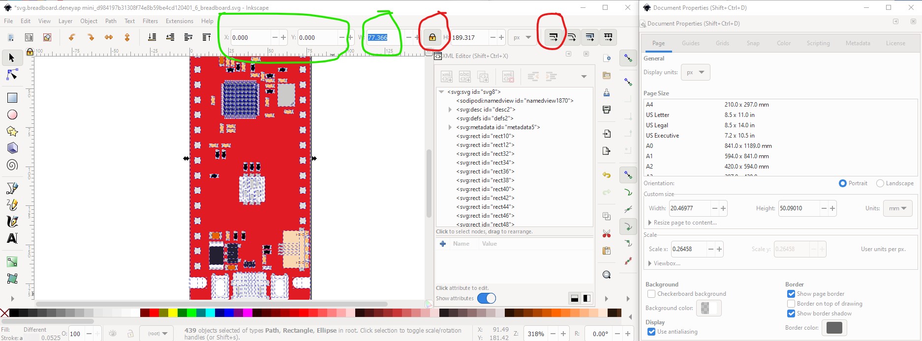
so do an Edit->select all then Edit->resize page to selection to get the svg correctly configured. Record the current width in px from the tool bar (we will need that to do the rescale) also lock height to width and set scale stroke width on rescale.
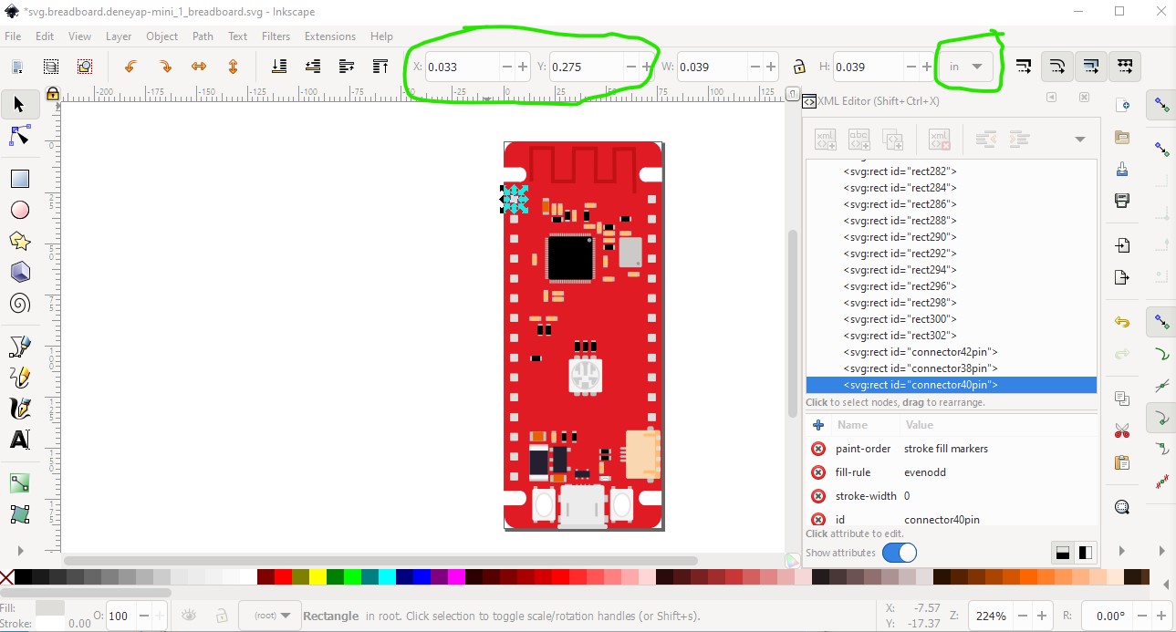
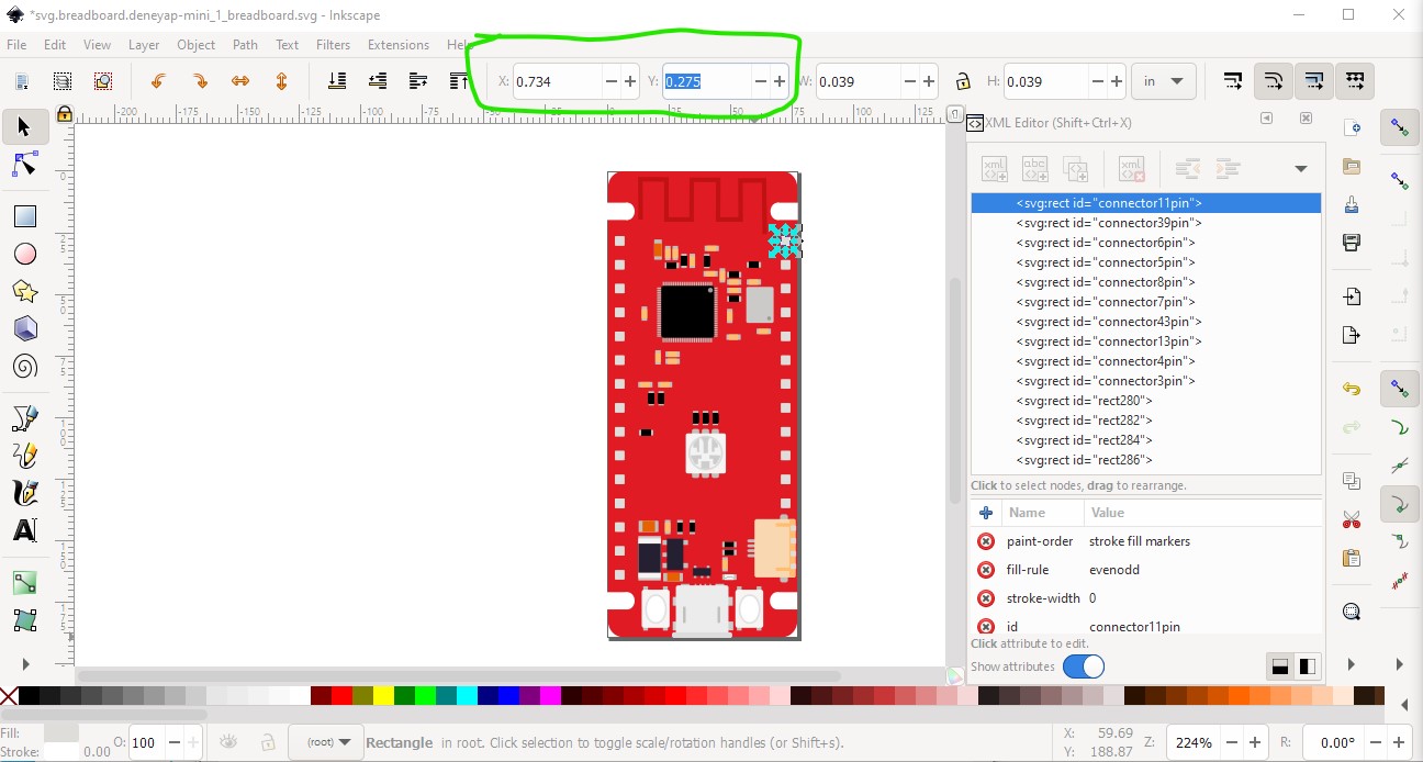
with the scale corrected now we reorginize and renumber the pins. First check the pins as an indication of the scale. The pins should be exactly on 0.1in boundaries but are not. Starting at connector0pin (top left) x 0.33in y 0.275in
changing to the top right pin we get x 0.734in y 0.275in. X on this pin should be 0.733in to match the left pin in X.
The Y axis is even furhter off. Switching to the bottom left pin we see Y is fairly incorrect:

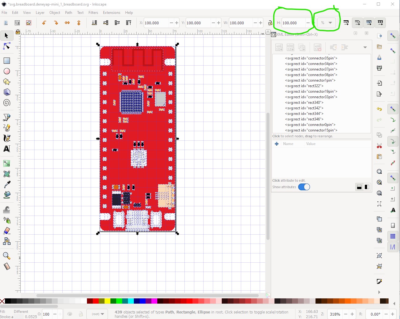
Here the pin is at x 0.033in y 1.686in when it should be 1.675in to maintain the 0.1in spacing. To fix this we need to rescale the Y axis until the connectors line up (which may make the size of the board incorrect!) In this image I added a .1 inch grid. You can see the top left connector has the grid line near the bottom of the square. The bottom left connector has the grid line in the middle of the square (when it should be in the identical place as the top.) The way to fix this is to scale the whole svg by the difference to bring the top an bottom connectors. The current difference between the top and bottom connector is 1.411in it should be 1.400in to be correct. Thus we need to reduce the scale in y to 99.22041105598866% of its current value. So Edit->select all do the entire image, then change the tool bar to % and set the height (Y axis) to 99.22041105598866%.
As we see that corrects the pins so they are exactly on .1in boundaries.

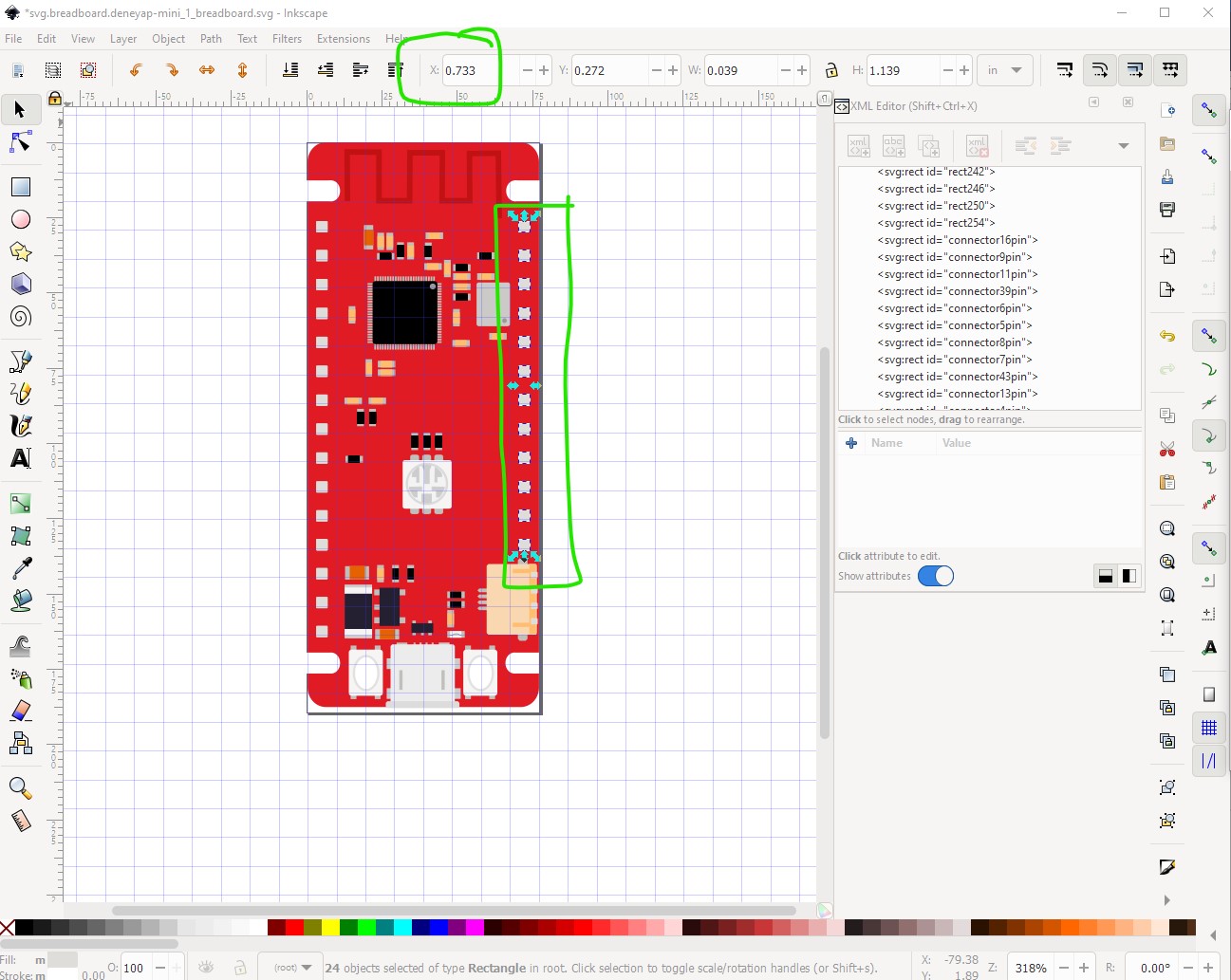
The top right pin is now x = 0.033in y = 0.272in

The bottom left is now x = 0.033in y = 1.672 in exactly 1.4 in from the top as desired. For the x offset it is small enough to just select all the pins on the right of the board and move them .01 in to align correctly.

and now the pins are correctly aligned as they should be.
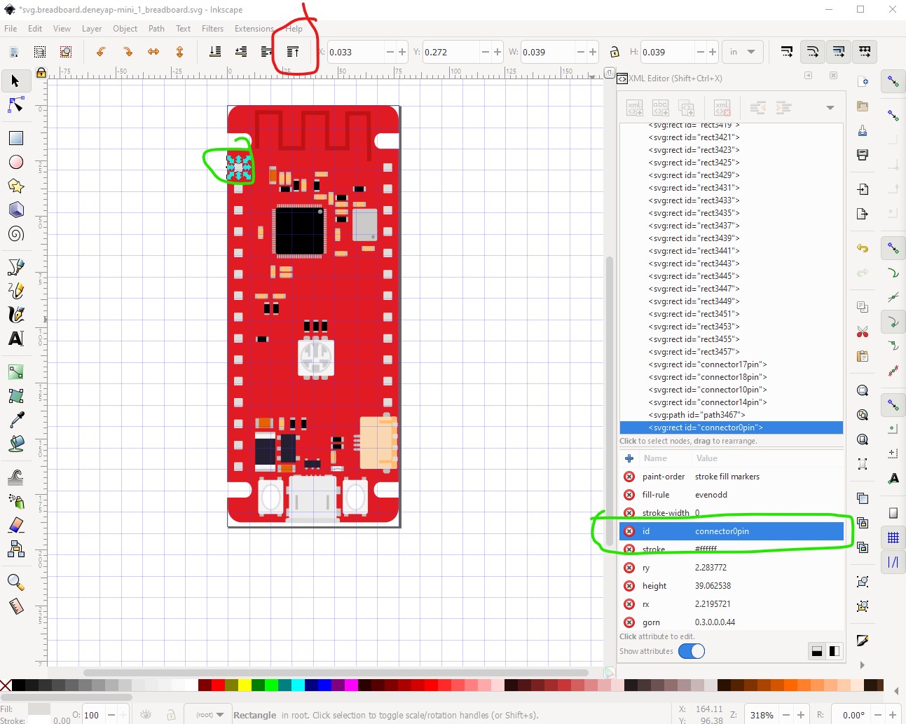
Now we need to renumber the pins to match the new fzp file. To do that I am going to move the pins in order to the bottom of the svg and then run a python script to renumber the pins. Since the script isn’t finished yet, you would need to manually change the id field on each pin to match the pin numbers in the fzp file.
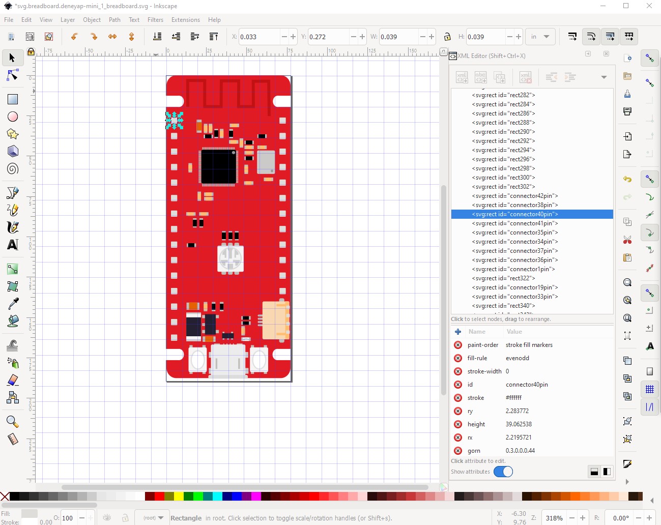
start with the top left pin (connector0) and move it to the bottom of the svg by clicking the nove to bottom icon (circled in red) and using xml editor to rename the pin from connector40pin to connector0pin.
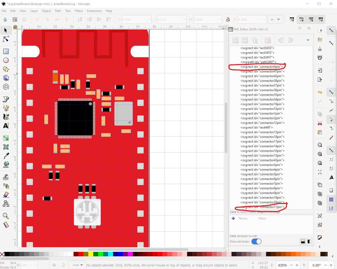
doing all the pins ends up with this.
For me I ran this
$ SvgSetConnectorsbb.py svg.breadboard.deneyap-mini_1_breadboard.svg
*** Process svg.breadboard.deneyap-mini_1_breadboard.svg ***
which produced this:

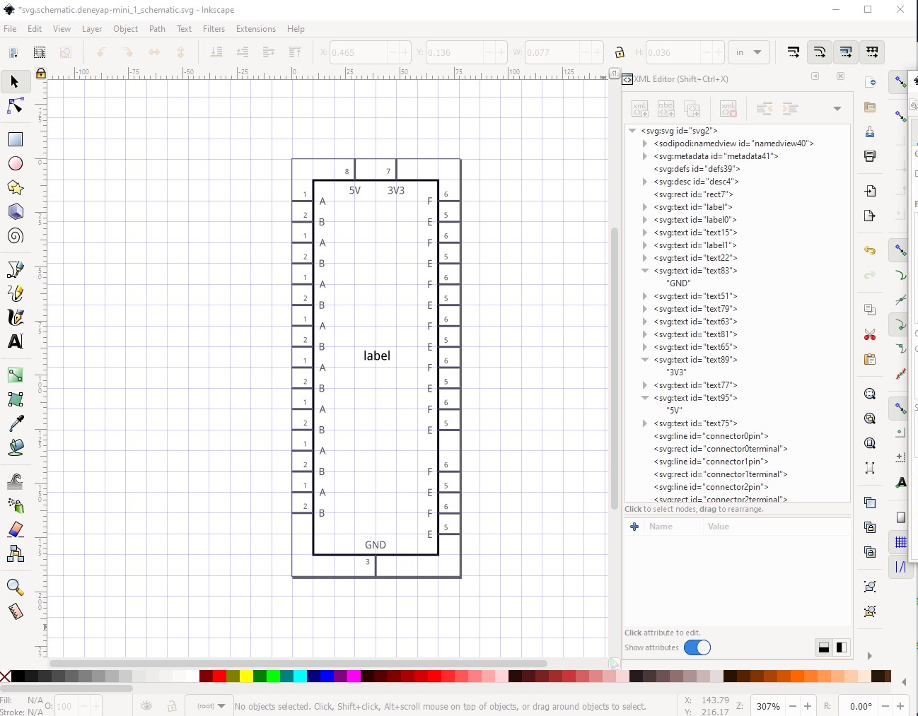
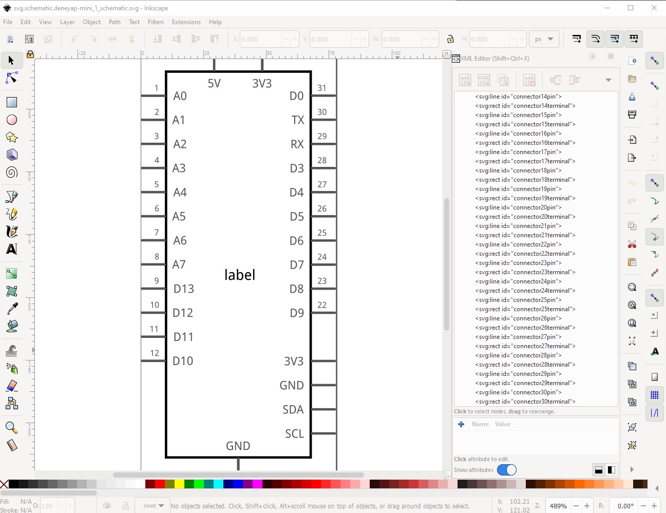
You would need to manually (either through Inkscape or a by running a text editor against the breadboard svg file) to arrange to change the Ids of all the pins in to this order. At this point breadboard is complete and Edit->Select all, Edit->resize page to selection, object->group rename the resulting group to breadboard and save as plain svg completes breadboard. Now on to schemaitc. A look at the current scehmatic tells me it will be easier to start from the schematic template (available in the tutorial post) so thats what I did. The starting template looks like this:

The two connectors on the top will be 5V and 3V3, one terminal on the bottom will be ground and the other deleted. The connectors on the left and right need to be expanded til we have enough connectors to fit all the pins. So set the tool bar to in, select the two left hand pins and duplicate them and move them down via the tool bar 2 spaces like this

repeat until we have 12 connectors (all the pins that are not 5V, 3V3, or ground) on the left side like this
also move the ground connector to the new bottom position (produced by increasing the height of the rectangle until its bottom is in the correct place.) Then move the power pins and the right hand connectors to their correct position like this
Now duplicate 14 connectors (all the right hand connectors that aren’ 5V 3V3 or GND unless they are part of the grove connector) to make the right hand connectors like this (with the 4pin grove connector separated by a space from the other right hand pins.)
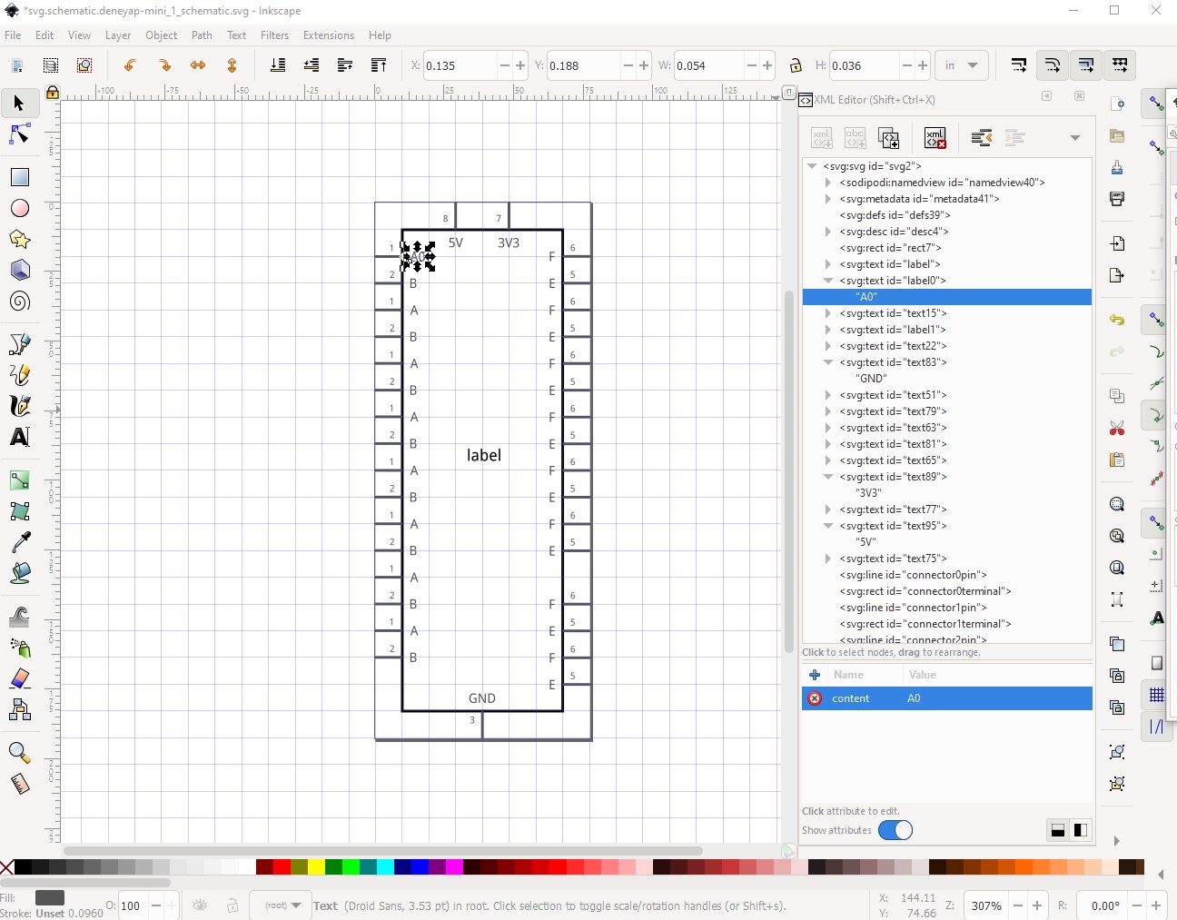
Now modify the text on the pin labels to match the connector number in the fzp file starting with connector0 at the top left.
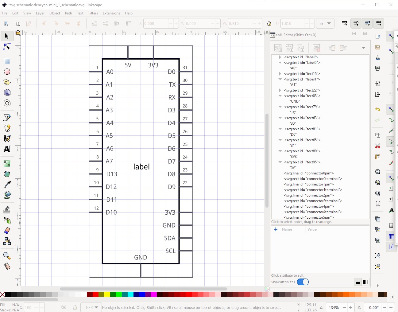
Doing that (and for now skipping 3V3, 5V and GND not on the grove connector) we come up with this
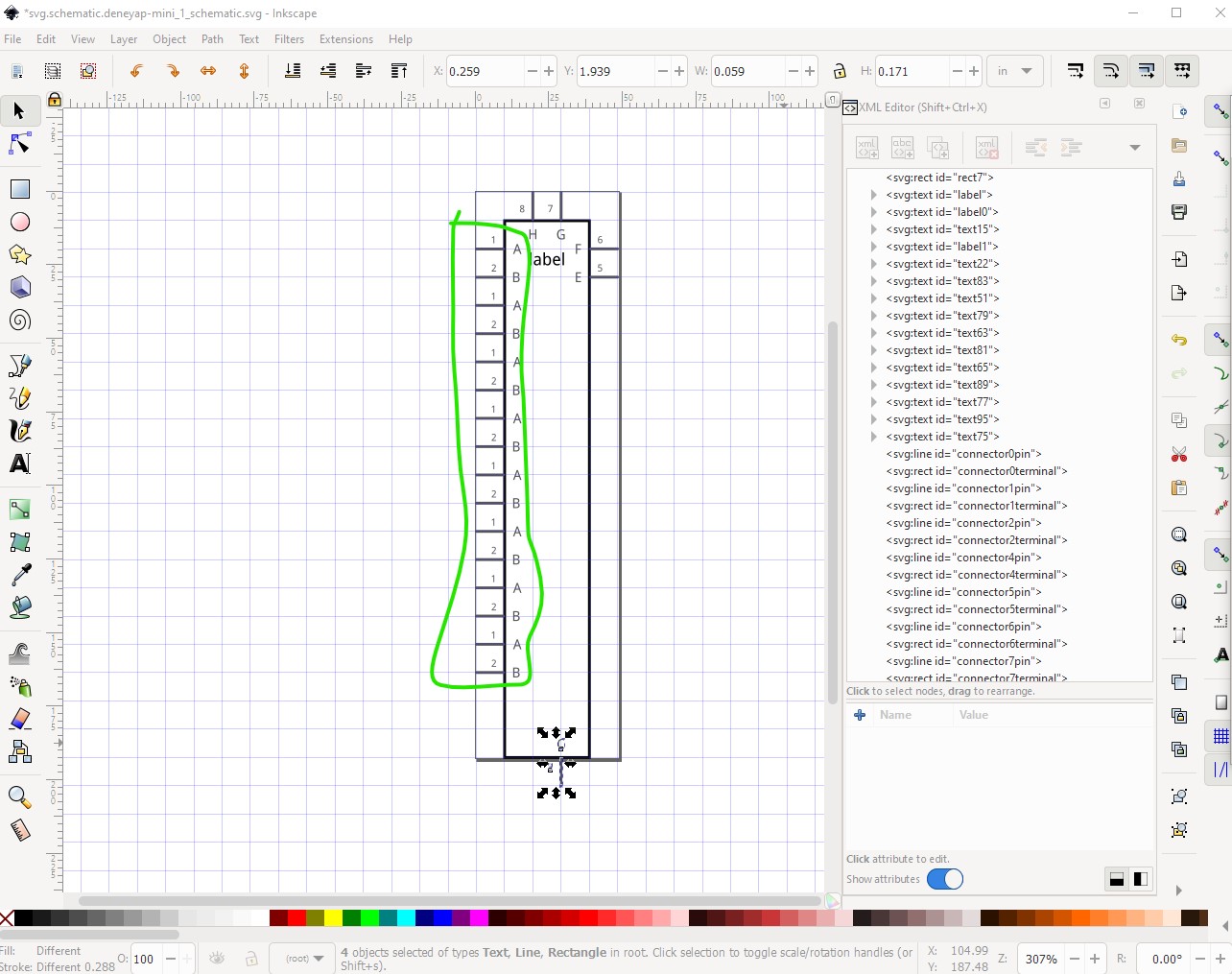
Now we need to start moving the pins in order to the bottom of the svg as we did in breadboard. Here there are two elements (the pin and its associated terminal) to move for each pin. Start with pin1 (connector0) like this
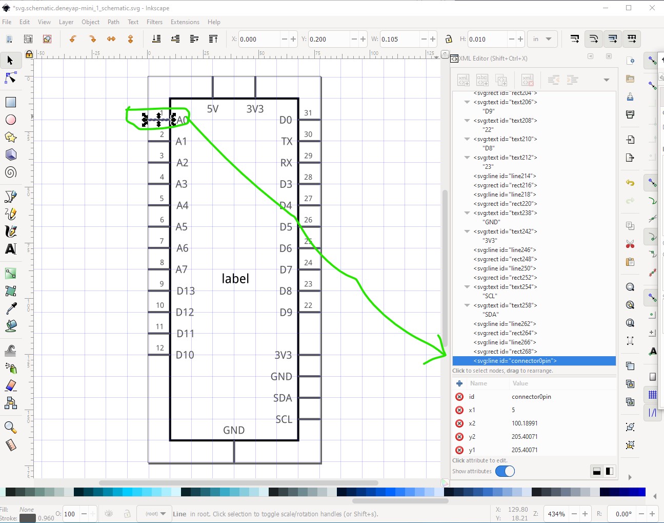
then its associated terminal
proceed with the next 11 pins in order
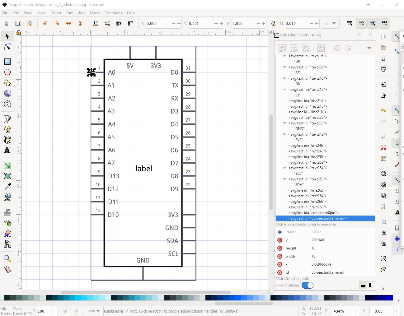
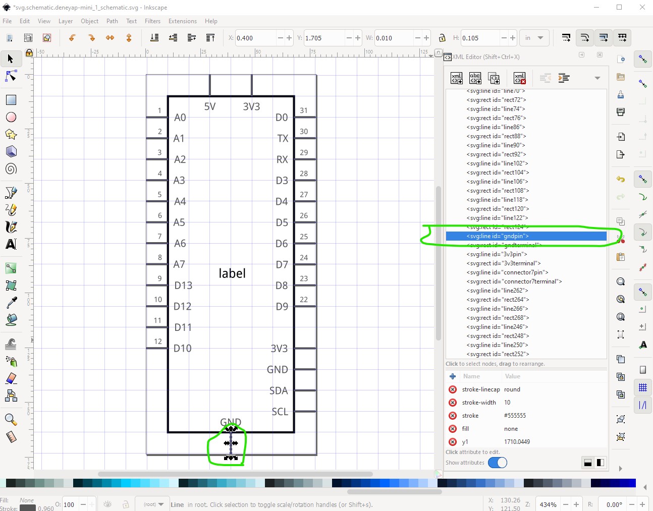
that gets us here, where things change (because the next pin is connector12 which is a ground pin and we need to do something different!) Connector12 (the next pin in order) is ground. So I am going to select the (so far!) only ground pin on the bottom of the image and move them both to the bottom of the svg as connector12pin and connector12temrinal, I am also going to change their names to gndpin and gndterm so I can find them later when I need another ground pin.
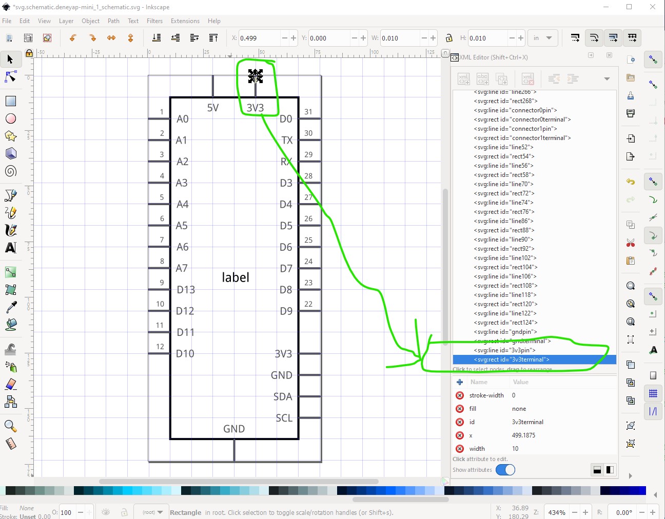
now on to the next connector which is 3V3. Same as ground, move the pin and terminal to the bottom and rename them 3V3pin and 3V3term
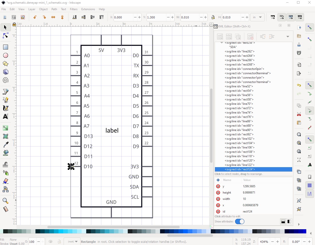
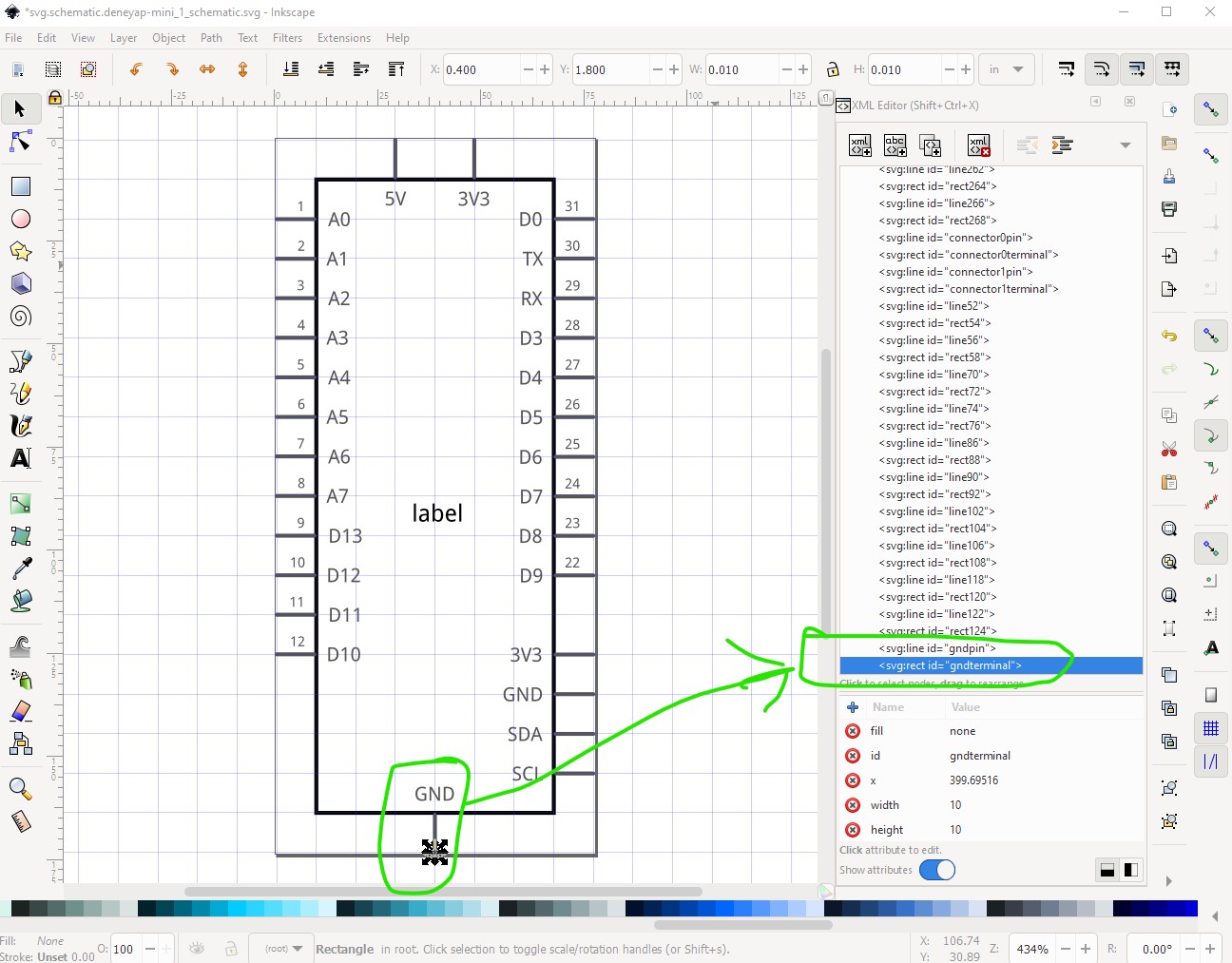
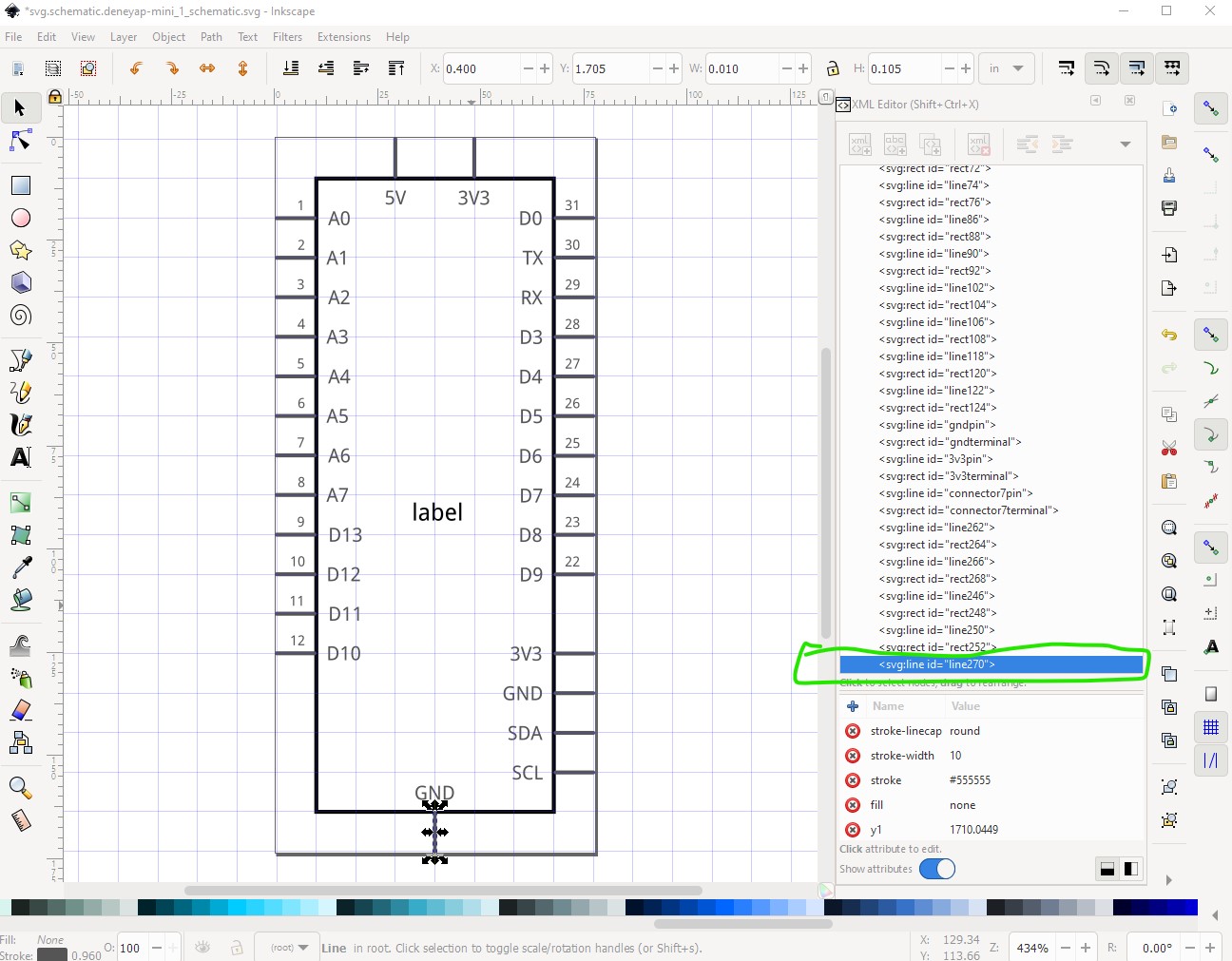
we are on a roll, the next pin is 5V but there is only one of them so it just goes to the bottom of the svg to be numbered in order, no renaming. Same with connectors 15 and 16 (grove SDA and SCL) just move them to the bottom to be numbered in order this contines with grove ground and grove 3V3 until we come to connector 19 which is again a ground but needs special processing. For connector19 (GND) we need to select the pin we named gndpin earlier and duplicate it (which will automatically go to the bottom of the svg), then do the same with the gndterminal pin. This creates a pin and terminal that overlays to original ground pin and terminal but will have a new connector number like this
duplicate the pin giving this
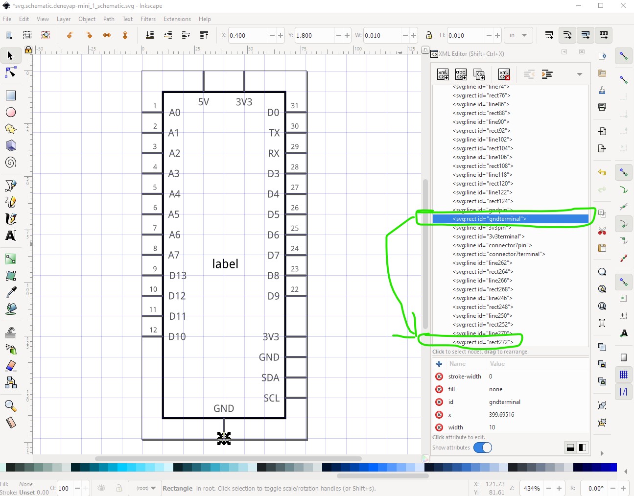
there is a new line (which will become connector19pin) at the bottom of the svg. Now do the same to gndterminal to make connector19terminal like this
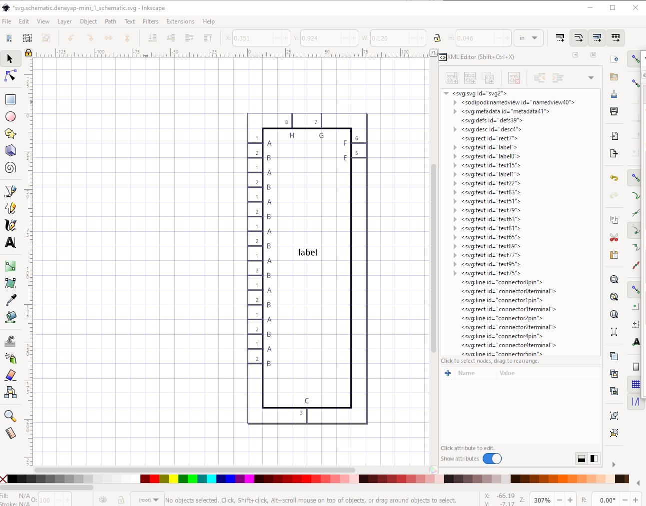
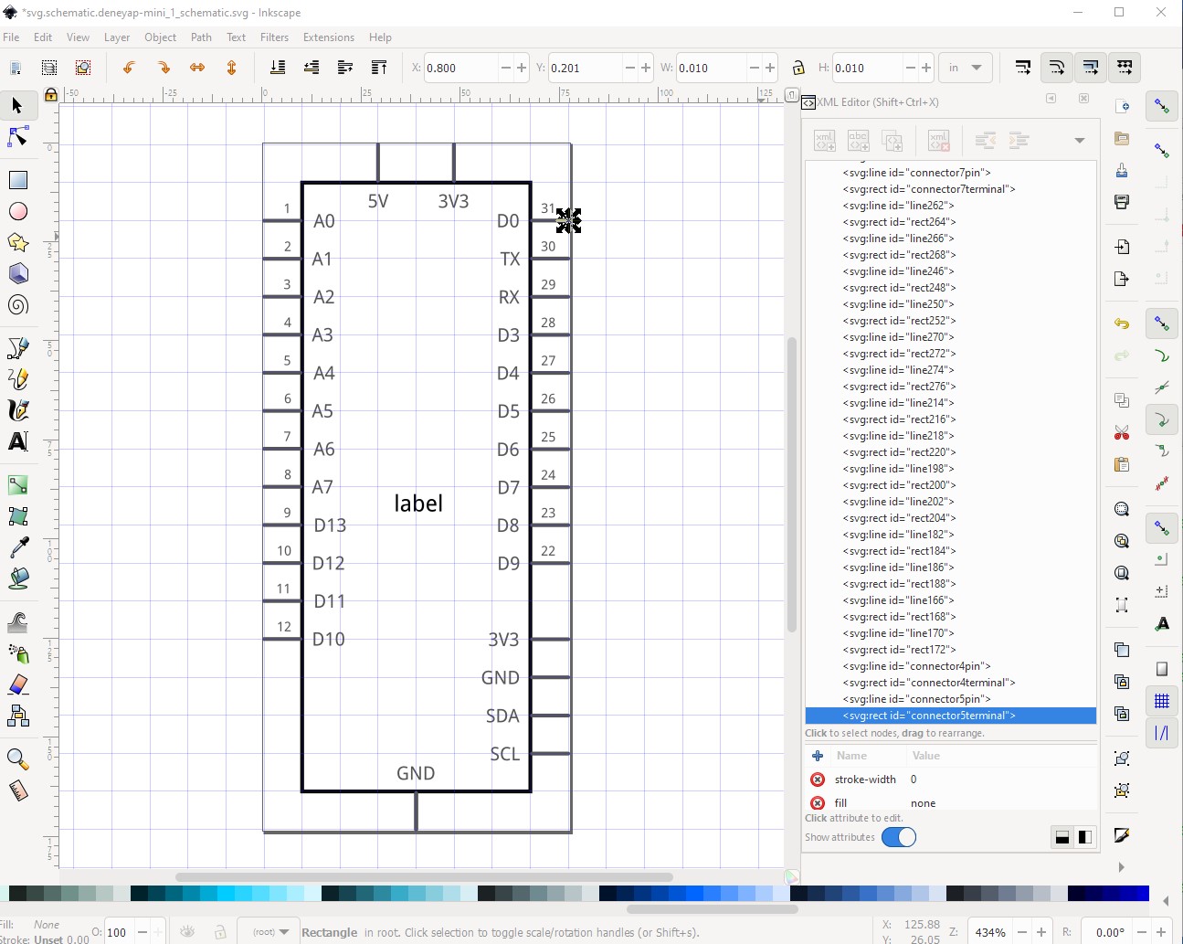
we need to do the same any time we come across a GND pin or a 3V3 pin in future. Connector20 is 3V3 so do the same as above with 3v3pin and 3v3terminal. Then proceed to do the pins in order up the right side of the image (D9 is next) until we have hit D0 at connector30. Then we are done and it should look like this
For me at this point I save the svg and run a script which renumbers the connectors like this
$ SvgSetConnectors.py svg.schematic.deneyap-mini_1_schematic.svg
*** Process svg.schematic.deneyap-mini_1_schematic.svg ***
which produces this
you are not as fortunate and have to manually renumber the connectors in to this order either using Inkscape or a text editor (either way a lot of work) until I manage to clean up the scripts and release them. In any case I can now do the usual Edit->select all, Edit->resize page to selection Object->group, rename the group to schematic and save as plain svg and schematic is finished. Now on to pcb. The current pcb is wrong, it doesn’t match the breadboard layout and is the wrong scale. So as with breadboard, ungroup it and rescale it as a start.
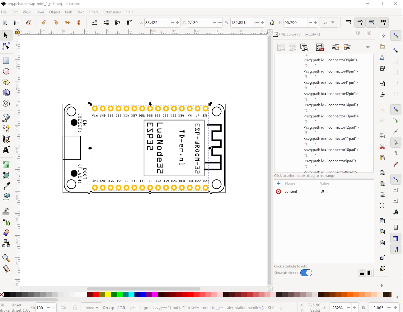
As it stands pcb is completly wrong. It has paths for connectors which are poor form (they work if correctly configured, which these may have been but are hard to modify and thus undesireable.) So to start copy the breadboard svg in to pcb to serve as the template like this
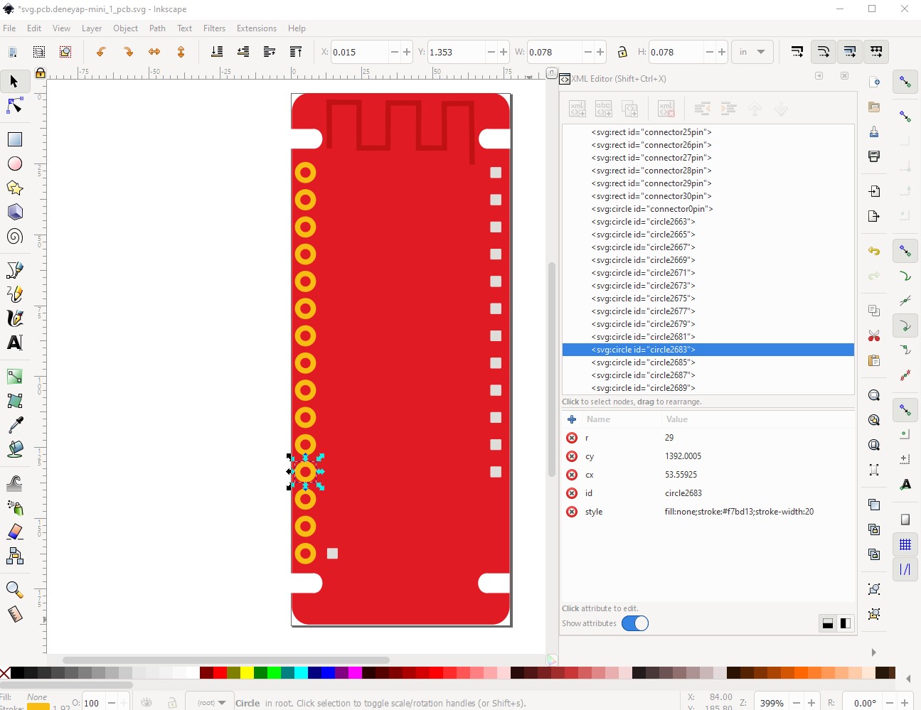
I don’t want any of the components or the grove connector so start by deleting all of them. Leave the antenna because it needs to be marked as a keepout area. Create a suitable pin for pcb, a cirle with radius 29 and stroke-width 20. This will give a pad with a hole of 0.038in suitable for mounting 0.1in headers. Now move that on top of the connector0 rectangle (which isn’t suitable as a pin in pcb!) to position it correctly like this change the Id of the cirle to connector1pin and delete the rectangle from breadboard. Delete all the pin rectangles except the bottom most one and move it 01in in x to be out of the way (but mark the last pad on this side.) Now duplicate the connector0pin circle and move them down .1 in to make the rest of the pads like this
ending up with this
The selected pad will be duplicated and moved across in X to become the right hand row of pads. Then adjust the stroke-width on the path for the rectangle to be 10 and set fill to none to change the path to the silkscreen outline.Do the same to the antenna to mark the keep out area for traces and the mounting hole slots. Note the slots will only be on silkscreen, if the user wants mounting holes they need to drag a hole over the mark on silkscreen to drill the holes. As with the other two svgs the connectors are at the bottom of the svg and for me are filled in correctly like this
$ SvgSetConnectorsbb.py svg.pcb.deneyap-mini_1_pcb.svg
*** Process svg.pcb.deneyap-mini_1_pcb.svg ***
Unfortunately I wasn’t careful enough when assigning the pin layout in breadboard and this creates the pin numbers incorrectly.
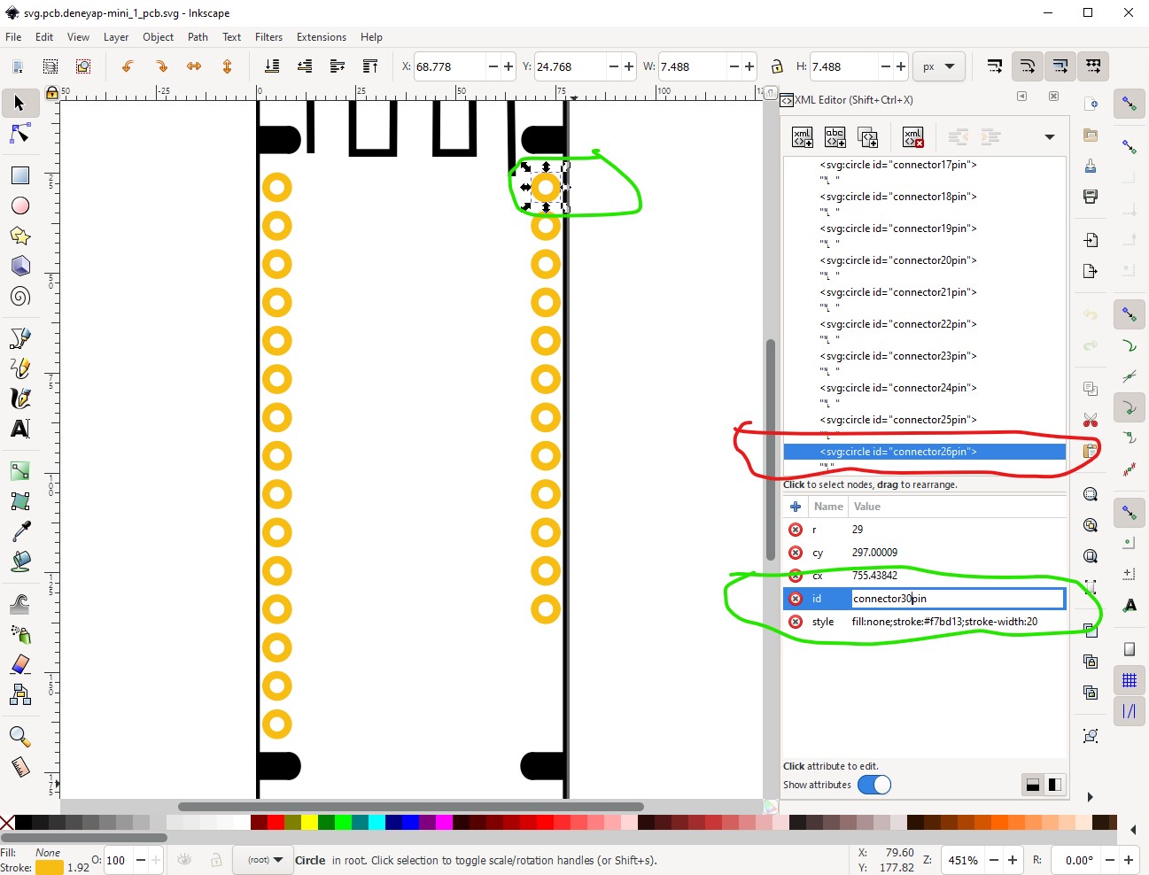
which creates this with the 4 grove connector pins missing
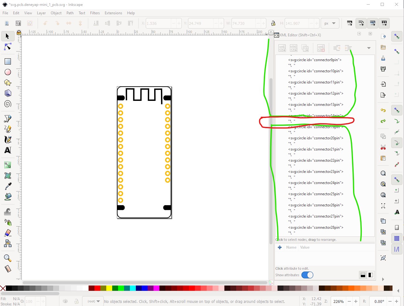
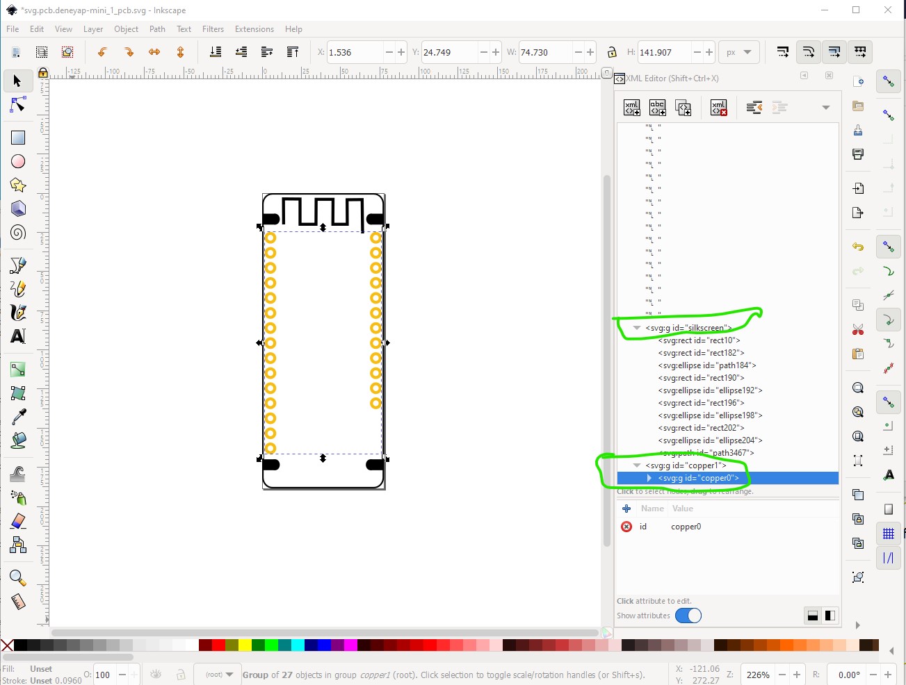
the red circle indicates that the 4 grove pins don’t appear in pcb and the pin numbers jump from connector14 to connector19 to reflect that. Now with all the pins correctly defined we create the necessary groups after the usual Edit-select all, Edit->resize page to selection to set the correct viewbox and origin. First we select all the pins and Object->group twice (to create groups copper1 and copper0)
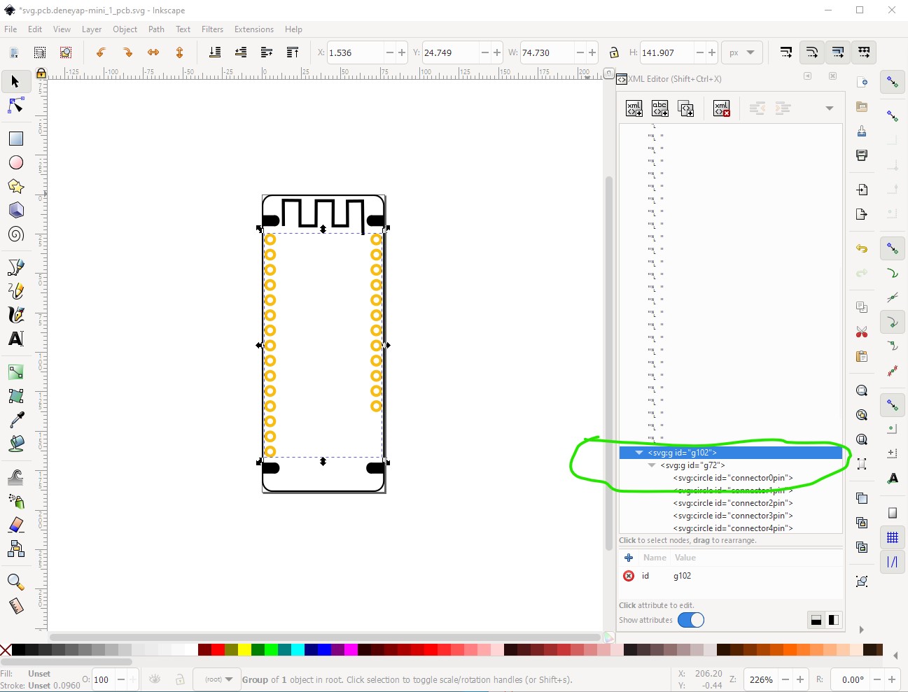
then do an Edit-select all and object->group to create the silkscreen group (which will contain copper1 and copper0 which we don’t want)

so select the copper1 group and unindent it in xml editor to move it back in to root where it belongs like this
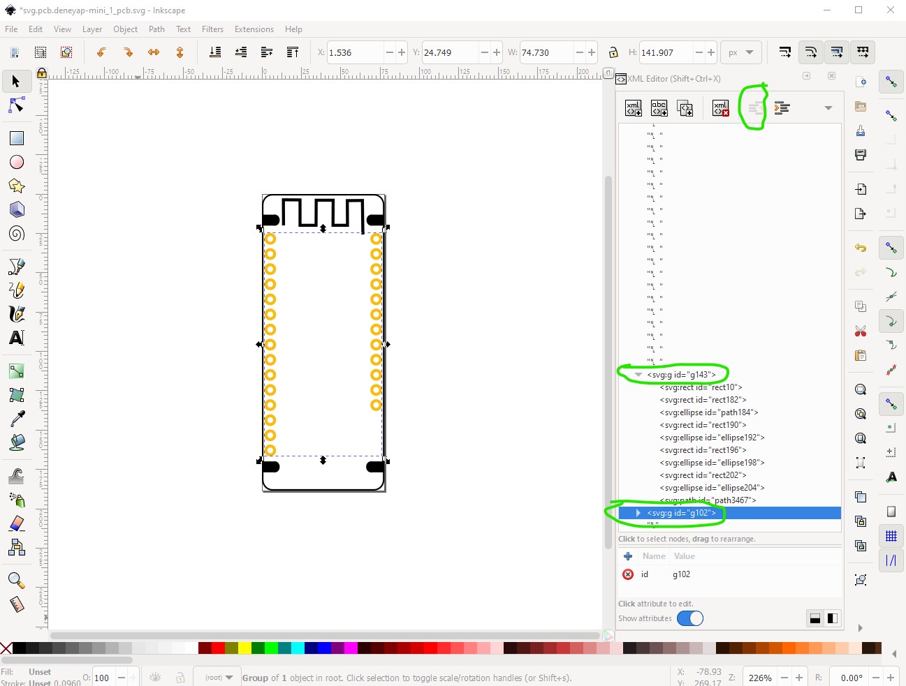
Now rename the groups to their correct values and pcb is done so save as plain svg and move on.
Now we need to modify the .fzp file to remove the pcb connectors from the grove connetor pins. We could use the inhibit keyword, but it has bugs around bussed connectors, so instead I am just going to delete the pcbview for the 4 grove pins like this. In a text editor (vi under cygwin in this case) find the first grove connector which happens to be connector15
  <connector id="connector15" type="male" name="SCL">
    <description>SCL (grove connector)</description>
    <views>
      <breadboardView>
        <p svgId="connector15pin" layer="breadboard"/>
      </breadboardView>
      <schematicView>
        <p svgId="connector15pin" layer="schematic" terminalId="connector15terminal"/>
      </schematicView>
      <pcbView>
        <p svgId="connector15pin" layer="copper0"/>
        <p svgId="connector15pin" layer="copper1"/>
      </pcbView>
    </views>
  </connector>
  <connector id="connector16" type="male" name="SDA">
    <description>SDA (grove connector)</description>
    <views>
Here I remove the two pcbview svgIdlines to leave this
  <connector id="connector15" type="male" name="SCL">
    <description>SCL (grove connector)</description>
    <views>
      <breadboardView>
        <p svgId="connector15pin" layer="breadboard"/>
      </breadboardView>
      <schematicView>
        <p svgId="connector15pin" layer="schematic" terminalId="connector15terminal"/>
      </schematicView>
      <pcbView>
      </pcbView>
    </views>
  </connector>
  <connector id="connector16" type="male" name="SDA">
    <description>SDA (grove connector)</description>
    <views>
repeat for the next 3 connectors and the .fzp and save the changes and the part should be done. So lets see if I screwed up by running the fzp file through FritzingCheckPart.py to see if it finds any errors. Yep I screwed a few things up.
$ FritzingCheckPartw.py part.deneyap-mini_1.fzp
… (unimportant notifications of changes)
Warning 19: File
‘svg.pcb.deneyap-mini_1_pcb.svg.bak’
At line 17
Height 188.4603 is defined in px
in or mm is a better option (px can cause scaling problems!)
Warning 19: File
‘svg.pcb.deneyap-mini_1_pcb.svg.bak’
At line 17
Width 77.759926 is defined in px
in or mm is a better option (px can cause scaling problems!)
Error 54: File
‘part.deneyap-mini_1.fzp.bak’
At line 535
Bus nodeMember connector19 already in bus GND
Error 18: File
‘part.deneyap-mini_1.fzp.bak’
Connector connector15pin is in the fzp file but not the svg file. (typo?)
svg svg.pcb.deneyap-mini_1_pcb.svg.bak
The pcb svg is dimensioned in px rather than in in which is wrong but easy to fix. Edit the pcb svg and change the dimension value to in like this
capture43.jpg
capture44.jpg
duplicate bus node member is also easy to fix (as the SCL def is wrong!)
<bus id="SCL">
  <nodeMember connectorId="connector15"/>
  <nodeMember connectorId="connector19"/>
</bus>
needs to be
<bus id="SCL">
  <nodeMember connectorId="connector10"/>
  <nodeMember connectorId="connector15"/>
</bus>
For connector15 I missed removing the pcbview definition in the fzp file so this
<connector id="connector15" type="male" name="SCL">
  <description>SCL (grove connector)</description>
  <views>
    <breadboardView>
      <p svgId="connector15pin" layer="breadboard"/>
    </breadboardView>
    <schematicView>
      <p svgId="connector15pin" layer="schematic" terminalId="connector15terminal"/>
    </schematicView>
    <pcbView>
      <p svgId="connector15pin" layer="copper0"/>
      <p svgId="connector15pin" layer="copper1"/>
    </pcbView>
  </views>
</connector>
needs to become this
<connector id="connector15" type="male" name="SCL">
  <description>SCL (grove connector)</description>
  <views>
    <breadboardView>
      <p svgId="connector15pin" layer="breadboard"/>
    </breadboardView>
    <schematicView>
      <p svgId="connector15pin" layer="schematic" terminalId="connector15terminal"/>
    </schematicView>
    <pcbView>
    </pcbView>
  </views>
</connector>
to correct that. Then FritzingCheckPart runs correctly:
$ FritzingCheckPartw.py part.deneyap-mini_1.fzp
**** Starting to process file Startup, no file yet
**** Starting to process file part.deneyap-mini_1.fzp
**** Starting to process file svg.breadboard.deneyap-mini_1_breadboard.svg.bak
**** Starting to process file svg.schematic.deneyap-mini_1_schematic.svg.bak
**** Starting to process file svg.pcb.deneyap-mini_1_pcb.svg.bak
File
‘part.deneyap-mini_1.fzp.bak’
This is a through hole part as both copper0 and copper1 views are present.
If you wanted a smd part remove the copper0 definition from line 52
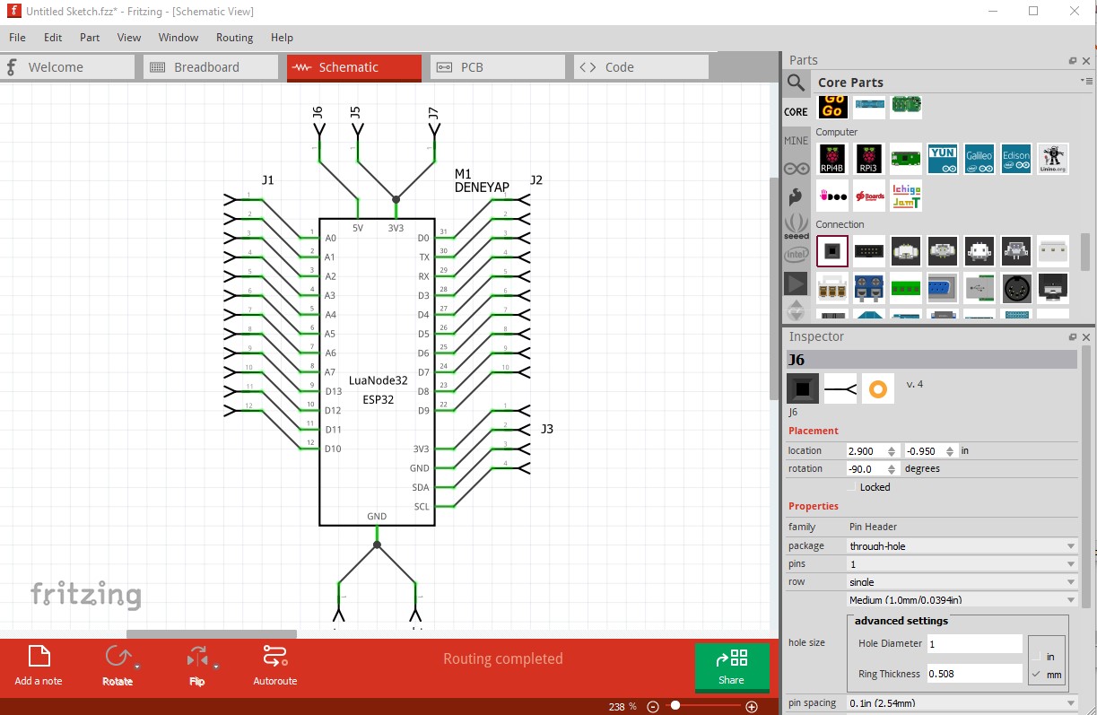
So now we can zip the files to make a .fzpz file and test the new part in Fritzing and check the gerber output for correctness. So load the new part in to Fritzing and start testing it. First check the bus connections are correct. Here I clicked on
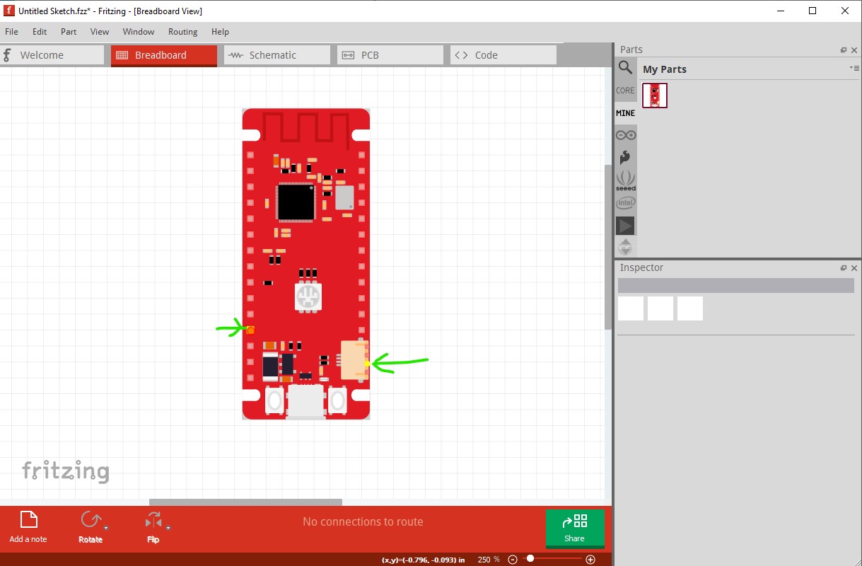
pin 13 (ground) and the other 2 grounds (on the grove connector and pin 20) light up yellow as expected.
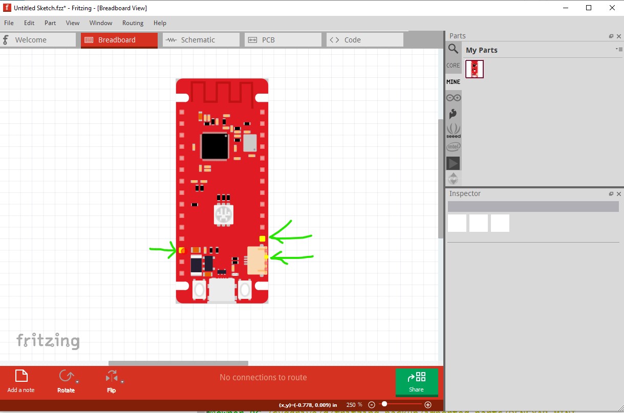
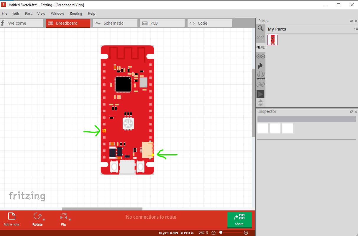
then click on pin 14 (3.3V) and make sure the other 2 pins light up yellow as expected
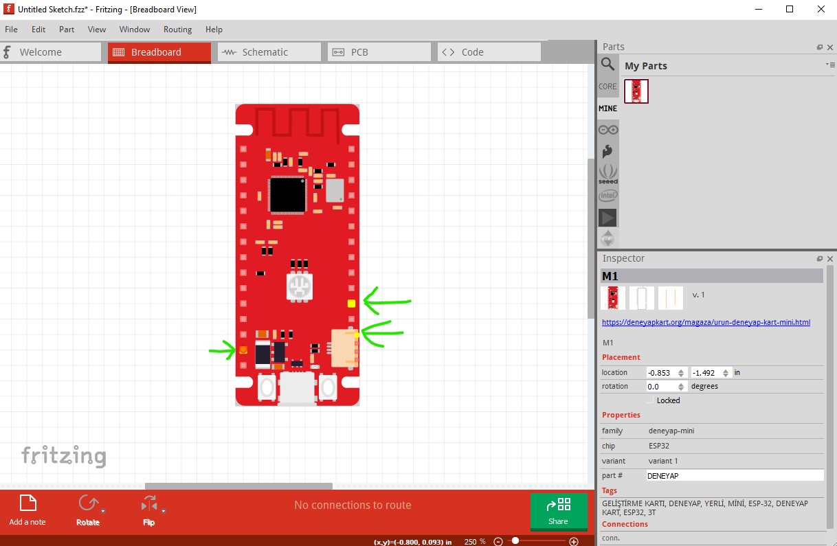
then click on pin 12 (SDA) and make sure it lights yellow on the grove connector
then pin11 (SCL) and make sure it lights up yellow on the grove connector
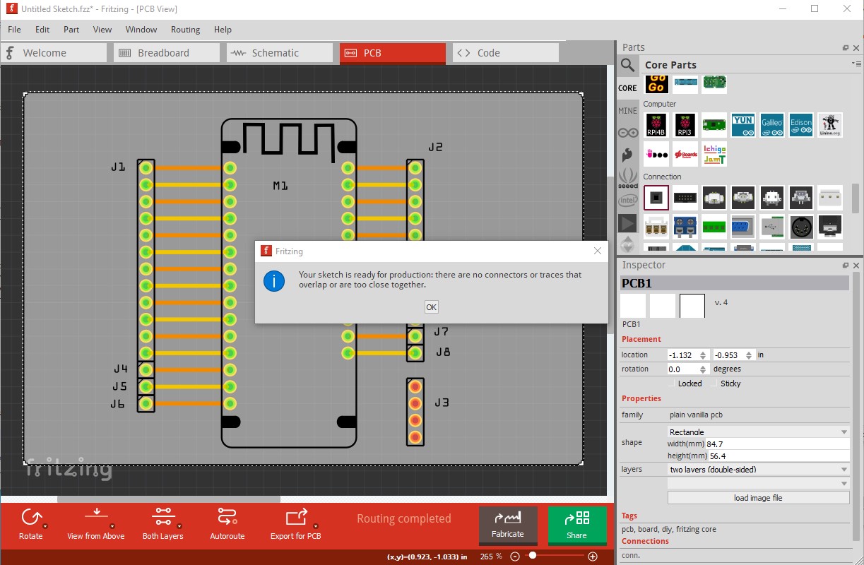
so all the buses look correct. On to pcb for a bit. Everything looks fine in Fritizng
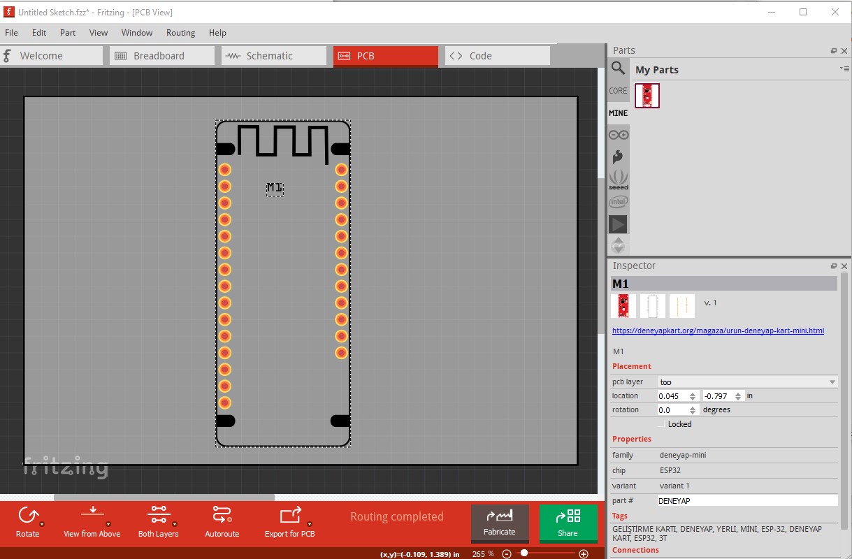
so export the sketch as gerbers File->Export->For production->gerber
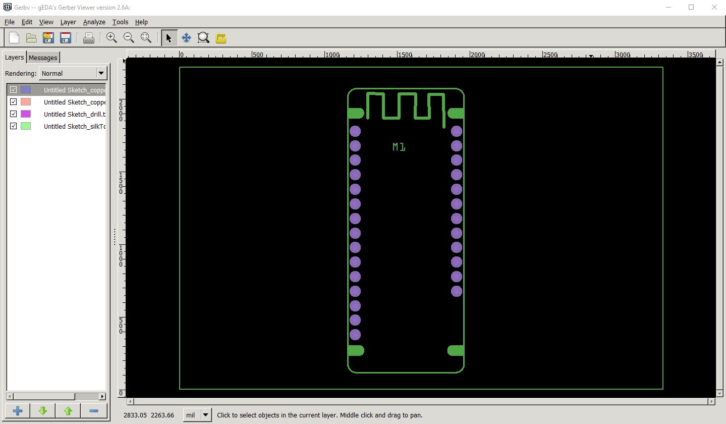
and view the result in the gerbv gerber viewer which also looks fine. On the way by I verified that the hole size is the correct 0.038in in the gerber drill.txt file. The reason to check the gerber output is that the pcb can look fine in Fritzing but still be incorrect in the gerbers (which is what the board is made from.)
Since there are no obvious problems, now move back to Fritzing and check all the connections for correctness. Drag in a .1 header and set it to 12 positions for the first 12 pins. Connect it up in breadboard and make sure the connections correctly reflect in to schematic and pcb (which they do here)
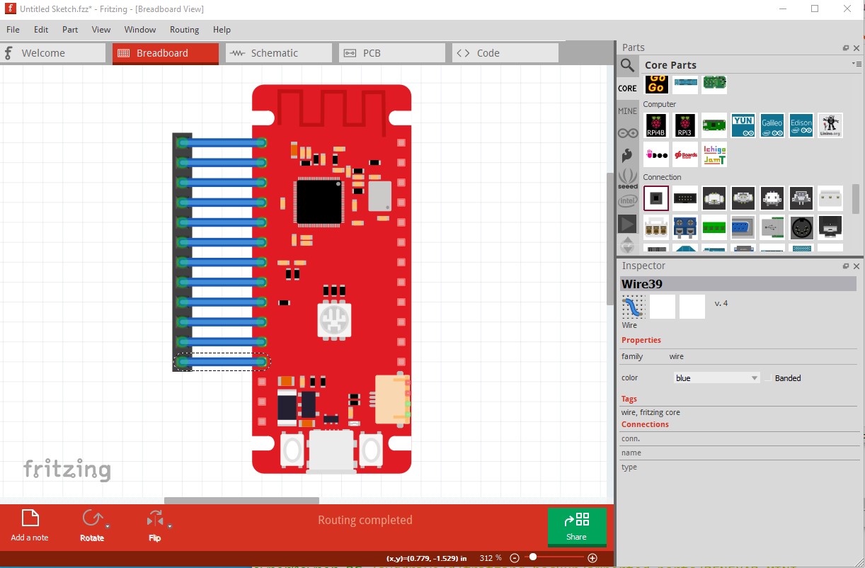

here in schematic the connections are at 45 degrees to insure the terminal is correctly set to the end of the pin.
Now connect single pin headers to all the power connections and check that they reflect in to the two other views correctly. Note the grove connector 4pin header has no connections in pcb (because we suppressed the pcb view connections in the fzp file!) Everything connects correctly indicating the part is correct.

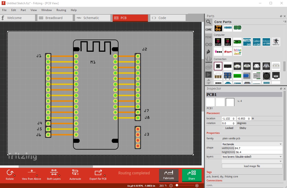
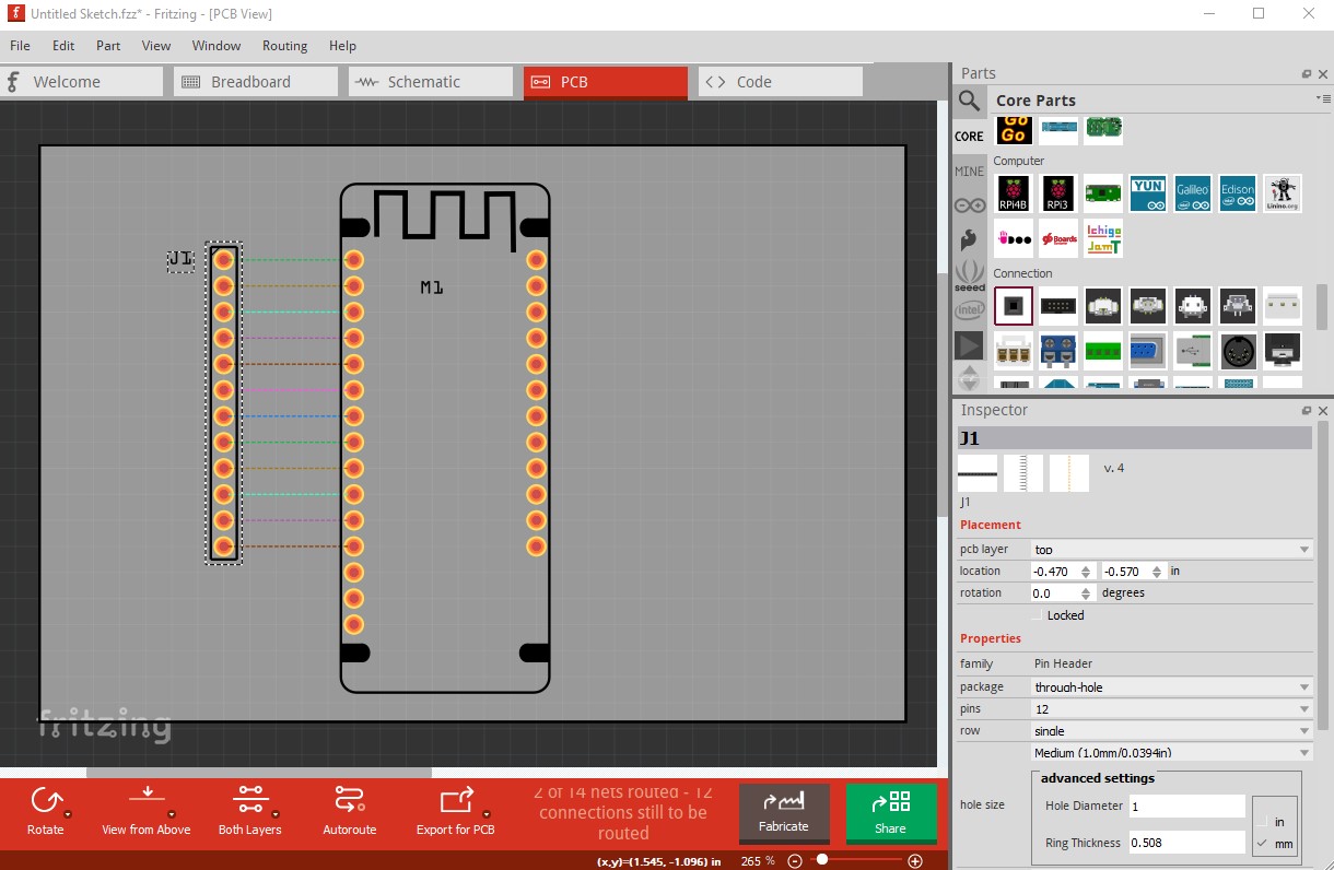
Note that I moved ever other trace in pcb to the top layer to make sure that both layers work in pcb. Now as a final check run DRC in pcb (Routing-> Design Rules Check) to make sure it passes.
Then export pcb as gerber and again check it in the gerber viewer to make sure there are no problems.
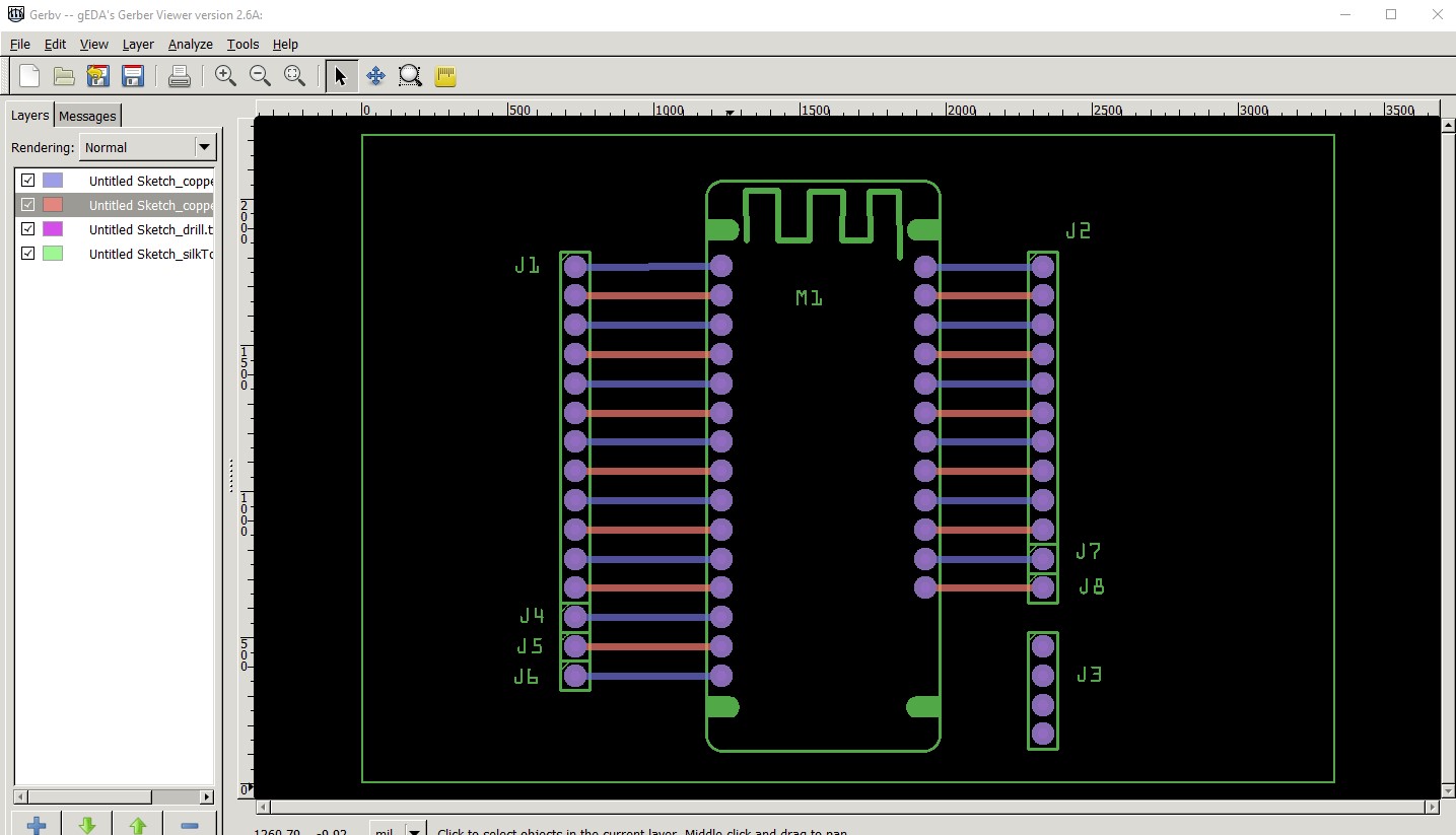
Since the gerbers look fine, declare the part correct and post all of this along with the corrected part. From this you should be able to do the same thing to the other boards you need.
DENEYAP MINI-fixed.fzpz (15.7 KB)
Hope this helps.
Peter
2 Likes