Ground fill thermal relief

After building a few boards, I’ve observed that manual soldering and rework of components connected to the ground plane is a real pain and takes special attention to avoid poor solder joints or components getting overheated.

I’m looking for a solution that allows me to use the ground fill functionality, since it makes routing so much cleaner, but allows me to decouple the pin/pad thermally for improved manual assembly/rework. Other CAD programs have ‘thermal relief’ or ‘thermal break’ or even copper fills that are a mesh fill instead of solid fill. Are there any similar features or settings in Fritzing? Any ideas on a workaround to achieve the result of thermal decoupling of the pad/pin from the large mass ground plane?

My initial idea was to surround my component with copper blocker, and instead of designating the component pins as ground fill seeds, route a regular sized trace a semi-short distance from within the blocker to the nearby ground fill. But i haven’t figured out how to connect the trace to the ground fill. When the plane is on the opposite side of the board, a via seems to work when set to ground fill. Although, i’ll need to test the effectiveness as a thermal break. Not sure how to make the connection when the plane is on the same side as the component.

Thanks
Chip

There are a couple of ways you can make a thermal relief… depending on what you are trying to do and if your board is DIY or fabricated by a PCB fab house.

The copper pad when commercially made will not be covered by a solder mask… The copper fill will be covered by solder mask. If you make as custom size copper fill and “lock it”, and then create another copper pour, the lock will keep provide a blockout around the custom fill. You can also use a combination of both pad and fill, like pad on top and fill on the bottom and connect together with vias…

You can create a custom shape like a pad or hole, make a copper pour, then delete the shape and lock the copper pour, create another copper pour and it will fill the void and create your shape out of with copper fill. Then lock the little copper fill custom shape and unlock the large copper pour and delete it. All that will be left is your custom shape. In FZ there is a work around for everything…

Another way is to make a custom part with copper pads on both sides connect by a bunch of laser drilled 0.33mm holes and insert it as a part. That is the way I normally do it. If the part requires a thermal relief, I will create a thermal pad in the custom part so that the thermal relief and connector pads are all together in the PCB view and don’t need the add it separately.

Fritzing has thermal relief. Right-click on part, Set Ground Fill Seed.

yep, i built a couple board designs with ground planes using that method, setting ground fill seeds, and such, and just letting fritzing make the connections to the plane. both for thru hole and surface mount components. problem is the pins or pads connected using the default settings are dang hard to solder to by hand. pretty much need to have the solder iron way hot and wait for ever to get a good solder joint. its not a show stopper issue, i was just wondering if there were some tricks in the board design process that would help make the soldering easier. I recently noticed there is a setting for the ground fill keepout distance or something similar. maybe that can be used to decrease the area used on a ground fill seed connection to a plane. lots of things still to investigate in fritzing for me. thanks for the input.

Isn’t this enough.
Set part - Set Ground Fill Seed.
Make - Routing/Ground Fill/Set Ground Fill Keepout, very big.
Then - Routing/Ground Fill/Choose Ground Fill Seeds/OK and ground fill.
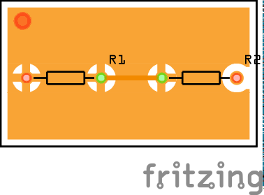
those are much larger than i have previously observed. i didnt change the keepout, so they were most likely set at default. will give this a try before getting more elaborate. thanks for the example.

It’s the Keepout that makes them big.

EDIT
To change it you have to Remove the Ground fill first before reapplying the new Keepout.

Not exactly sure what you are trying to accomplish, but here are some tips and tricks you can play with…

First: if you don’t have a temperature controlled soldering iron, you need to get one. The irons with a lamp cord you plug into the wall just don’t work. My suggestion would be one of these, http://www.ebay.com/itm/2-in-1-Soldering-Rework-Stations-SMD-Hot-Air-Iron-Gun-Desoldering-Welder-852D-/181139781537?hash=item2a2cc5b7a1:g:xC4AAOSwMgdXxAUc , If you do have a temperature controlled iron, it is always handy to have a second one. You can keep them set up different with different tips…

Second: Use a small chisel tip, they retain more heat and have better heat transfer than a little pointed tip. Make sure you have a little solder contact between the tip and copper for better heat conductivity…and always flux… I prefer the no-clean type. Use leaded solder, easier to work with than unleaded. Set iron temp to 330c for leaded 350c for unleaded. Watch some Youtube videos on soldering tips and tricks… The hot air is extremely useful for SMD, pick up small syringe of leaded solder past. Solder past can be used with the iron or hot air. Watch more Youtube…

As for Fritzing, you can always insert the vias after the copper fill, then you don’t need to set the ground seed. You can place a pad or hole where you don’t want copper fill on the board, set the copper pour, then remove the pad/hole, you now have a custom keepout. You can connect a trace to copper fill after the copper fill had been poured; draw a trace from the pin/pad/via to another pin/pad/via, put a bend in the trace and delete one end of the trace by clicking on “Delete Wire up to bendpoints”, the free end can now be dragged any where you want… If you want to split the ground plain in half or section off the ground plain; place two vias on the board, or off the board, draw a trace between them, pour the ground/copper fill then delete the vias…