If the original poster made the changes I suggested above they didn’t post a new version of the part. That said, your new version still has a number of problems, mostly cosmetic but the pcb hole size is only 0.036in and they need to be 0.038in to fit 0.1 header pins so your new board probably won’t work either. The breadboard svg is still missing its layerId and thus won’t export as an image.
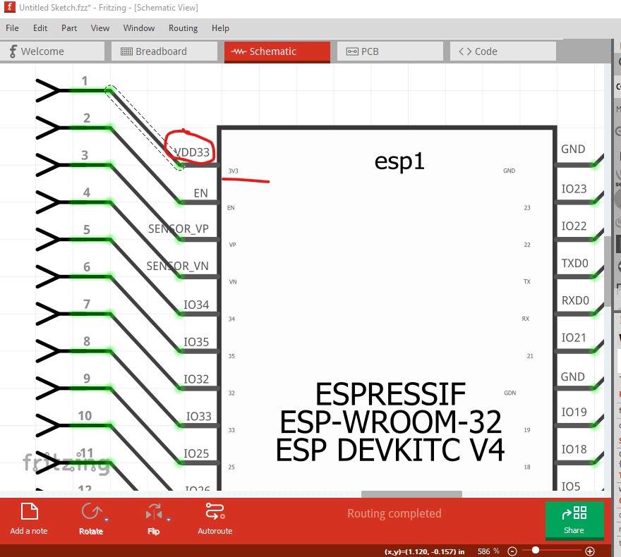
In schematic the problems are cosmetic. The font sizes are wrong, the one circled in red should be 35px and be the pin number and the one beside the pin should be 49px and the pin name. In pcb
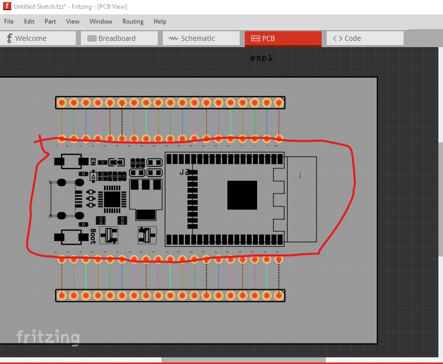
all the stuff and pin numbers should be deleted, the outside edge of the board should be 10 thou wide and be the outline of the complete part and as noted the holes in the pads should be 0.038in like this (taken from the gerber output drill.txt file)
; NON-PLATED HOLES START AT T1
; THROUGH (PLATED) HOLES START AT T100
M48
INCH
T100C0.036000
T101C0.038000
%
T100
X010125Y007051
X025126Y007051
X007125Y017055
…
T101
X015126Y020051
X011126Y020051
X007126Y020051
the line T100C0.036000 indicates that the holes defined as T100 are plated through, and 0.036in in diameter. The T101C0.038000 indicates that the T101 holes are plated through and 0.038in diameter (and are the 0.1in headers I added to the sketch!) Here is a corrected part that meets the graphics standards and is ready to be added to core parts.
ESP32_DevKitc_V4.fzpz (37.9 KB)
Peter