That’s so weird I was just wondering about trying just that. Will let you know if it works!
Even when I rotated the copper pad on the right side 180 deg. it didn’t work… The right side of the blocker/copper has to be touching the board… weird!
1 Like
It’s a go! Have and a excellent day and thank you for making these files!
Can I get a more n00b-friendly explanation for how this works?
I’d like to import a custom shape (like a logo) that blocks out the soldermask.
1 Like
Hi Steelgoose,
Can you give a quick rundown of the steps you used to create a custom solder mask keep-out shape? I would like to do more complex shapes.
Thank you,
E
Hello, yes can you explain a little bit more about the process ?
Thank you
Best
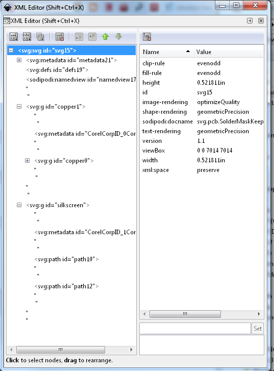
Actually the secret to invisible copper is fill=none, stroke-width=0 or stroke=none. The fill=none causes the copper to not render (as there is no fill), but the solder mask code is obviously not checking (either intentionally or more likely due to an oversight) for fill and creates the solder mask for the invisible copper, doing what @steelgoose wanted by exploiting what is probably a bug.
Peter
1 Like
I guess these are the settings for the svg file but how do you turn this svg file into a custom fritzing part in this case (especially starting from an IC)? Thank you for your time!
For me (who doesn’t use the parts editor), I unzip the fzpz file to break out the 5 files (a fzp and 4 svgs), use Inkscape to make the necessary change to the the pcb svg (called svg.pcb.Part-name_pcb.svg) then rezip the 5 files in to an fzpz and test it. If you are using the parts editor, I believe you will change the pcb svg and then reload it using the parts editor (I can probably figure out the exact details if required.) From a recent post I wouldn’t try exporting the file as and svg from parts editor, it appears the export mechanism is broken (at least for the Raspberry pi) as it doesn’t export the svg correctly. A better bet is to right click on the part you want in the parts bin and hit export part which will write the part as an fzpz file ready to be unzipped (I use 7zip).
Peter
1 Like
Thank you so much for your answer! I’ve had big troubles with the part editor so I will try your approach.
Thanks a lot again!
Unfortunately the parts editor wasn’t completed when development stalled in 2016 so it has issues in various places. I have never managed to make the connector assignment work for me (despite Old_Grey’s videos on how to do it) and only use it to generate new unique moduleIds and sometimes to change the meta data (although I also know how to edit that in the fzp file and often do it there.) As long as you know what the xml should look like I find it much easier to do the editing directly. Feel free to post if you have questions or problems (preferably post the svg or part you are having trouble with), always happy to help people make good parts.
Peter
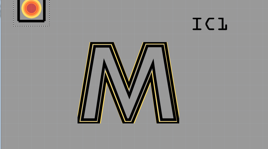
So I tried over 30 different versions but it unfortunately didn’t work. Or at least, it doesn’t seem to work when I view it from a gerber viewer:

I designed the svg in illustrator, following the same structure as the svg from @steelgoose file. Then I went to a file editor and added the height and width in the svg file. I then started a new part from an IC and imported this svg in the pcb view.
In the SVG, the fill is set to none for the path which is in the copper0 and on fritzing it also looks empty. However, the gerber viewer looks different.
I think it’s time to give up. I’ll try to to this on eagle probably… Thanks for your answers however.
Here’s the part I end up having if anyone’s interested
nathan.fzpz (5.3 KB)
I was just about to ask for that when you posted it  . I can see your problem, the path is not invisible:
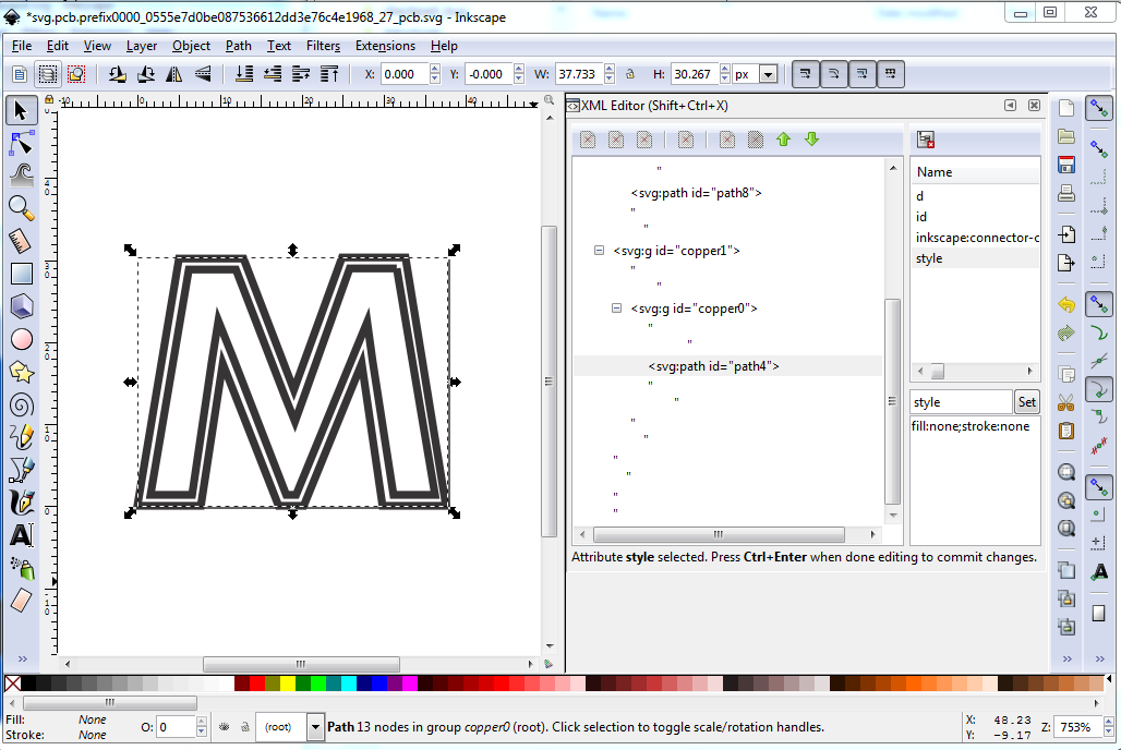
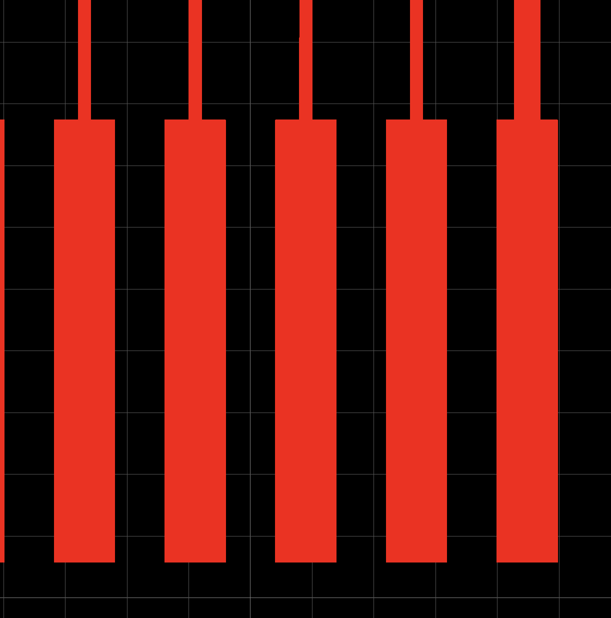
This is Inkscape rather than Illustrator, but it shouldn’t matter. The dark lines in this won’t block the mask, only an element that exists in copper but has neither fill nor stroke will work (and that is probably actually a bug). The masker assumes it is copper and blocks mask and silksceen but the gerber copper output doesn’t think it is copper and doesn’t generate a trace (thus “invisible copper”). It looks like the gerber code is deciding the whole M is not copper (which is probably true.) Here is the gerbv output of only the top mask layer:
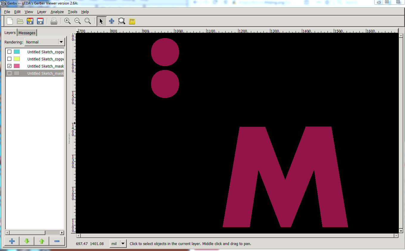
(I added a two pin connector to give the gerber code something to generate because gerbv wasn’t happy with just the M without drill layer.) I’m not clear on what you are trying to get though, do you want just the M without solder mask on top and bottom, or do you want copper (unmasked) on the M. I suspect you may need to use rectangles rather than a path to get what you want, but that may just be my ignorance of paths. Fritzing appears to think there should be copper (which isn’t translating to the gerber) around something (perhaps silk from the black) although it isn’t really clear.
I’d expect the gold parts to be copper, but gerbv doesn’t agree.
Peter
Hi steelgoose,
I’m using your ‘240x150 solder mask keep out’ file on a project (slot riser for Apple II).
It first glance it seems to work very well…
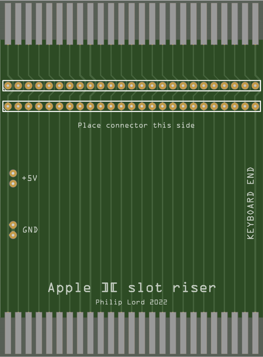
…but when I view the PDF in detail I can see a fine line in the “etch copper bottom” and “etch copper bottom top” layers that represent the outside parameter of your ‘240x150 solder mask keep out’ file.
I’m assuming this isn’t a good thing as it’s potentially connecting all the fingers for the edge connector together.
I know it’s a big ask, but would you be able to have another look at the file and see it it’s fixable?
Much thanks.
Philip

steelgoose hasn’t posted in several years so I doubt you will get a reply. This may be an artifact of pdf production, does the gerber output show the same problem? If you upload the sketch (the .fzz file, upload is 7th icon from the left in the reply menu.) I’ll poke at it and see if I can find a fix.
Peter
Hi Veneer,
Yes, I think you are correct. I opened the grebes in a gerber viewer and I am not able to see the line(s). So as you suggested, it’s probably a PDF render artifact. Thank you very much.
That likely isn’t fineable without a code change, your best bet would probably be to use something to edit the line out of the pdf. It may be easier to export it as an svg instead of pdf and edit the svg in Inkscape though.
edit:
Two solutions occur to me, assuming you are home etching, don’t bother with the solder mask blocker, you won’t have solder mask to worry about (unless there is some new way to apply solder mask to home etched boards?) The other is to extend the size of the blocker past the ends of the board on the assumption that the pdf code is reacting to the edge definition of the solder mask blocker (although that is essentially the same as omitting the solder blocker.) A third option is to define the pins on the edge of the board as connectors by making them a custom part. As connectors they won’t have solder mask but the traces that connect to them will (I’m assuming the edge connector pins are not defined as Fritzing connectors here!)
Peter