The overview given at http://fritzing.org/pcb-custom-shape/ is a good start, but I believe it’s a little outdated and missing a couple of important details.
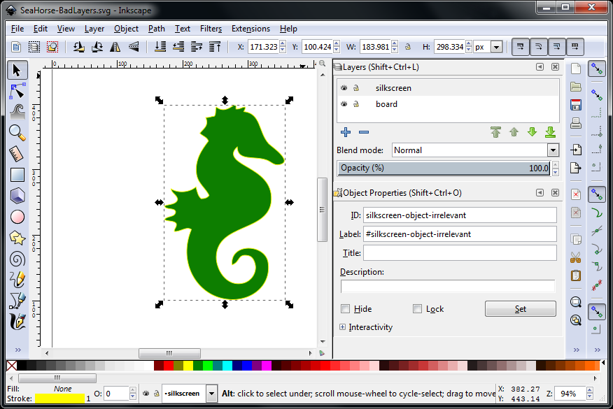
The instructions on that page say at the bottom to set the ID to “board” and “silkscreen” in Object properties or the XML Editor, However, it’s the layer that needs those IDs, not the Objects. I usually set the Object ID to something related for clarity, but it’s not even necessary.
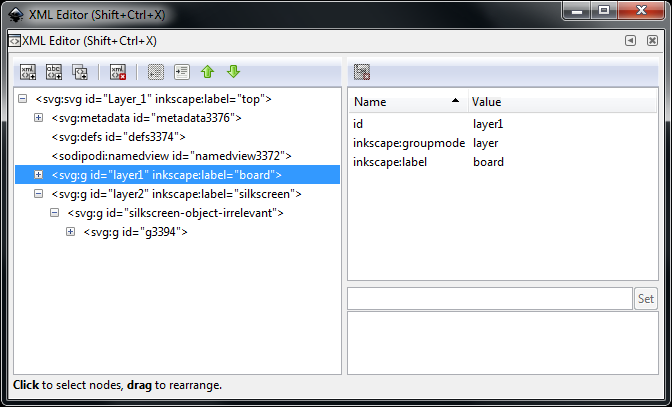
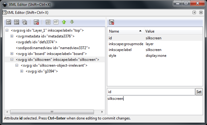
So even though the layer names appear right, Inkscape has an internal naming scheme represented in the XML, Fortunately, Inkscape lets you edit the XML of your SVG file directly. Just click Edit->XML Editor.
See how the layer names we set are stored in inkscape:label? This is wrong.