Now that I’ve mentioned to ‘Good’ parts about ground fills, let’s move on to the ‘Bad’ parts…
In order to create ground fills, the first step is to run traces connecting all the ground connections on your board. Then you select the ground net as the seed for the ground fill and add in the ground fill. At this point, I got to looking around at the PCB and noticed problems with the ground fill. See here:
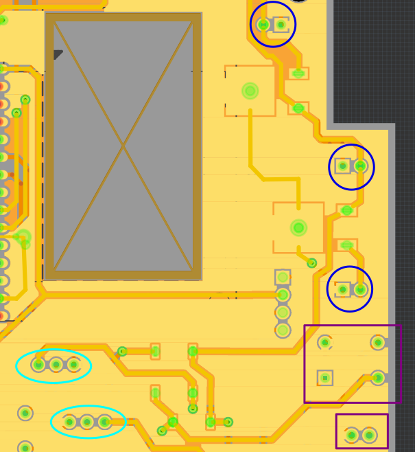
The three blue circles are electrolytic caps, standard fritzing parts, and all connected to ground. The top and bottom one has ground fills connected to the square pads, the middle one doesn’t have a ground fill connecting it. It only has the routed trace connecting it to the ground fill.
The 2 light blue circles are fritzing transistors and they are connected correctly.
The 2 purple square boxes - one is a 2 pin header, it connected correctly. The other one with 4 pins is a custom part (downloaded from the forum) and it’s connected correctly. 3 other custom parts missed getting nice ground fills connected to them. So some fritzing parts work with ground fills, and some don’t. Some custom parts work with ground fills, and some don’t.
Routing connections to ground fill islands can be a bit challenging. Take this example:

The big green circles are the connections to the ground fill. The little green circles by the big green ones, that your connection point. It’s not on top of the circle as I would expect. This is a minor problem.
At the top of the pic, I have one 16mil trace connecting two ground fills by going between pins of an ESP32 breakout. I clearly have room to run 2 more traces between the pins of the ESP32, but it appears I can only run one trace from connector to connector. Running 3 traces from connector to connector would be better than 1 trace, right? Same thing goes for the lower part of the pic, I could have used 3 traces instead of one.
Another issue I had was the ground fill connectors. Twice, the ground fill connectors were right where I wanted to place a via, making it hard to connect the two together. It would be really nice if one could move the ground fill connector like one does with a components silkscreen label.
At one point, I realized I needed to shift some traces around to connect 2 ground islands together. I moved the traces around, deleted the ground fill, and created a new one using fritzing’s PCB Copper Fill tool. This tool is in the Core part’s PCB View, drag it onto the PCB to fill an area. Drop the top-right corner of the square on the area you want filled. This worked well for that case…
When I deleted a ground fill that covered 3/4 of the board and tried using the Copper Fill tool again, it didn’t work. Not really sure what went wrong there. It just didn’t generate the fill.
Kinda like sticking your fingers in an electrical outlet as a kid. OK, that shocked me, so don’t do it again
Up next, the ‘Ugly’ parts of ground fills,
Randy