Confused about New Part Fab

I don’t think it is necessarily the parts that are wrong. In breadboard LED2 is shorted (by a rats nest line) which indicates a bad connection in another view. Here the anode of the LED connects to pin 2 of the optocoupler but a rats nest line shows a short (from a incorrect connection in another view.)

capture

in schematic the anode of the LED is connected to the resistor rather than pin 2 of the IC thus creating the short.

When I delete both wires on the LED the correct rats nest lines appear from breadboard (and the LED needs to be flipped 180 degrees to connect correctly.)

dragging a wire from the cathode of the LED to pin 5 of the optocoupler will cause the short we saw. The correct thing to do is to do the wiring in breadboard then click in the rats nest lines in schematic and route the resulting wire correctly (as it will make the correct connection from the other view!) In pcb the LED is set to SMD and it appears that you used vias an pads to make a through hole part. A better bet is to change the LED to through hole in Inspector which will create the pads you want like this.

a better bet would be this

change the package in Inspector (lower right window) to THT like this

then route the traces directly. If you click on the package line in Inspector it will give you a list of the packages available. This one is for a 3MM through hole LED. Then back to schematic where the unrouted nets message indicates another problem.

The rats nest line shows a short across the switch. This is because of an incorrect connection in breadboard reflecting in to schematic.

This wire is incorrect, when I delete it the correct connection shows up as a rats nest line

although there is still an error somewhere as routing hasn’t completed.

moving the diode up one position causes routing to be complete except for pcb which still has unrouted rats nest lines.

Peter

Hopefully I am not so confused with all your help. I have another version that was designed for
my Knife Steel surface grinder. ( I am a Blade Smith so have to flatten forged steel ) This one
utilizes a similar circuit and program but has more toots and whistles. It has similar limit switching, and has a separate step controller for the Large stepper that it has to interface with.
[ direction of desired travel ] That will be optically isolated, not shown in MY circuit.
I changed out the Limit Switches due to failure to route, used Reeds instead, worked perfectly.
This circuit also has 2 OVER RIDE push button switches for one axis for set-up or correction.
The Arduino Uno Part has a similar problem as the actual unit. I have a programmed call for
A5 to light a diode (started out in program as something else that physically failed) and the schematic did it faithfully, however the PC board layout had other results. The last pin on the
Arduino is marked SCL, and pin A5 is marked as A5. Since it’s an obvious discrepancy, I would
like you to check the Arduino Fritzing Part. All other pins routed correctly. I used only parts that gave me no problems and /or replaced the ones that did, so routing went relatively smoothly,
and repairs were minimal. [ the ANALOG pins in this unit were re-defined as DIGITAL I/O ]
The board Traces were manually routed for this go, and oversize “Pads” ( you have another name for them) were inserted for Arduino and TB6600 inter-connections. The components
and remaining Rats Nest were maintained for checking purposes against my operational
bread board Model and wiring diagram beside me. I have 3 type Optical isolator circuits
for impending machine isolation of other functions that do very little in this Board configuration
but are necessary for my equipment interfacing. I will try to send the latest Proto-part
to at least show you the I/O difference.
I could not find reference to addition of "OFF BOARD Equipment hook-up so manually added
“Pads” and traces to have a soldering point for those. As I have time, I hope to find hints in the
forum to assist me in future projects.
Bill
Surface-Grinder-Isolation-WithTB6600-MOTOR-DRIVER.fzz (187.2 KB)

I just ran AUTOROUTE on the manually drawn board I fabricated from the routing lines.
I only saw it pick up the 3 jumpers I had put in it earlier.
Bill

There isn’t anything wrong with the limit switch in your original circuit. It should route just as well as the reed switch. If you can upload a sketch that shows the incorrect routing of the limit switch I’ll see where the problem lies (as it doesn’t seem to be the switch part!)

The Arduino part is working as designed. The SCL pin on the Arduino connects to A5 internally (you can’t use both pins at the same time because they are internally connected.) In this image I clicked on the SCL pin at the top of the Arduino, as you see that A5 pin on the bottom also lights up because the two pins are internally connected. Fritzing routing will go to the closest pin in the same net. So a connection to A5 that is nearer the SCL pin will route to the SCL pin. You can fix that if desired by manually routing the trace to the A5 pin, but the autorouted solution is likely shorter as Fritzing selects the shortest route.

There isn’t directly an off board connection option. The usual solution is to use a generic header of the correct size like this. Here I dragged a generic header in to pcb (along with an Arduino Uno) and set the number of pins to 6 in inspector.

then in breadboard I set the header in the path of the wire to the Arduino like this

note you need to drag a wire from the Arduino to the pin header and from the breadboard to the pin header in order to get them both to connect, and thus it may be better to put the header in the breadboard like this

as it is less prone to missing connections. On the original if you move one of the wires on the header it will likely disconnect the header which will disconnect the header in pcb if you don’t notice it. As you see from the yellow dots the ground is connected to both the header and the Arduino. In pcb the header appears as pads and will connect to ground because it is in the ground net

In pcb I would suggest routing all the connections to make sure they all go where you expect. However there is a problem with that (which I currently can’t figure out!) If I right click on the wire I should be able to move it to the top layer (necessary because the off board wires cross each other!) But for at least some of the wires I can’t

This wire for instance won’t move to the top layer when it should. This wire however will move to the top layer (as the other one should) and I don’t know why there is a difference, as the board is two layer (even though all the traces are on the bottom layer!)

and the wire will correctly move to the top layer.

I can’t see (and don’t know of any setting that will do this) how some wires are only bottom layer. It makes me wonder if you have database corruption again (although this is a very odd form of it!)

Peter

Thanks Peter, The PCB IS a double layer and I did not realize it for several hours.

I only laser expose, or negative / Positive expose on one layer, since I have not found
positive acting in 2 layer with DATAK demise. I do get some materials from MG.
The reason my board REMAINED 2 layer is that after 4 hours work, I attempted to
Change it BOTTOM Single layer … did not file ( I know better ) and I lost ALL my work when
Fritzing CRASHED ! Haven’t tried it since. I will attempt it on a new project with no work
performed on Start. Working at home in the basement, unless I make a jig, and run boards
on CNC or Laser, I cannot match up delineation targets of opposing sides.
Other solution is to drill 2 holes and put board on them for location.
(CENTERED and Dimensioned )
I read about the inter-connection in programming, but had not run into it until yesterday.
( Arduino was not too clear of actual connection, I just thought it was a programming note. )
The assembled bread board runs fine as wired, and I had no reason to test the SCL polarity,
I don’t use it. The “CLOSEST” feature BITES ! I BIT ME.
If you know anyone making their own Surface grinder or similar X-Y machine, and wants to
use an UNO+Stepper Driver, I can forward the file if you have a way to do this…your forum
does not accept ZIP from here. I think my board is ready to burn a proto-type for testing.
Bill

One other item: FLATCAM opens Gerber, Can make images easily and other output files.
Found it while looking for Fritzing Drill conversion to GCODE. Seems to do quite well
with Fritzing Gerber output. It writes DXF.
Bill

The crash is a bug. I’ll try and reproduce it here (should be fairly easy) and file a bug report. Crashing and losing work is undesirable. Fritzing usually leaves a backup file around (with a date and time file name as I recall) which has at least most of the work though, but not crashing is a much better option. It is possible that the attempt to change from double sided to single has corrupted your .fzz file which may indicate problems too.

A trick to get a zip file uploaded is to rename it to .fzpz (which is also a zip file) which will upload. Then add a note the the .fzpz file is not a part but rather a zip file so people know what it is and don’t try and load it as a part.

Peter

I just tried to recreate this, and a couple of resistors with traces between them works fine. It converts to single sided and back with no problems and no crash. There looks to be something else going on in your case. I just tried your sketch above and it too converts to single sided without issue, so I don’t know what was going on there. Converting it back to double sided has not cured the “some traces won’t change layers” issue though. That appears to be because the routing database is again corrupted. Here I deleted all traces in all views and moved the breadboard (so there are no connections in breadboard.)

but there are still connections in schematic and pcb (just not correct ones!)

in both cases they show nets still to be routed when all the nets should be gone. Since you are the only person I have found who has managed to create more than one corrupted file I have a request (which is likely to be a lot of work though!): could you keep a log of your actions when making a sketch? What I need but have never been able to find is a list of the actions that cause the database corruption. As noted you are the first person I have found that has managed more than one. That says to me something in your workflow is tripping the bug and if we can get a record of the workflow we may be able to finally fix this problem! Another possibility is a custom code build that will record the redo log (which will allow the recreation of the sketch) to a file. That code doesn’t currently exist, and I haven’t done anything about it because this hasn’t been reproducible but since you seem to be able to cause these that may be a worthwhile change to make.

Peter

 I shall try to keep on top of it for you on my next project. This file was copy of the earlier project because the TB6600 had been updated, and the earlier limit switches were working after Your update, I DID have problems with the limit switches and diodes, so exchaqnged those parts, so I chose to leave those parts in the file and pretty much have a starting file just like the one YOU just showed.. All parts imported or duplicated, just lying around on screen waiting to be used. I try to create them in ORDER of the naming convention, However, I DO Edit and change the names to make logical sense. ( maybe Fritz has a problem with NAME changes. )
I actually did NOT check if schematic had residual components after cleaning the file for recreation of the Surface grinder...just proceeded to design Breadboard to look like the one on my desk. ( I will in future though  - I use a lot of Arduinos )  I destroyed 3 Arduinos on my own breadboard by bumping or dropping a bare leaded object on them and creating an 

Electrical SHORT! ( Smoke Test the HARD Way ! I HATE BREAD BOARDS !! )
Wires and components have different diameters and refuse to stay in or make contact…
take me back to the WIRE WRAPPING Era. (1970’s) I ordered a dozen SCREW TERMINAL adapters for Arduino UNO. I already have them for NANO. I only use MEGA for actual CNC/3D Printers, and some engraver operations, so THEY are soldered.
I do not plan immediate development (Ground-Up) of new projects for a while, I have Physical
developments I have to address to make spending cash.
Bill

I was just talking with the lead developer on github and it appears that saving the redo data base is a problem. Apparently the coordinates in use are local to the sketch and can’t be exported in any useful format. I had suggested this as useful data in an earlier go around on this particular bug. He did point out that we have an undo history available in Window-Undo history

I have asked if we can easily output this as a file (which I expect we should be able to) as it may provide some clues to what is going on especially if we can output the full log from the start of the sketch. During that discussion I have discovered that I need to in fact delete the breadboard not only move it (moving it apparently doesn’t remove the connections from the routing data base, but deleting it does!) So I’m now looking at replacing your pads in pcb with single pin headers which should to the same thing. It will look like this in breadboard

like this in schematic

and like this in pcb which may or may not equate to J2 here (they are both grounds though)

I’m hoping that will give me a sketch without routing corruption which I should then work correctly in pcb to make sure that everything works correctly… Your current sketch may have problems due to the database corruption.

Peter

Sounds like it. That should work great, Everything I construct is basically Machine Control most
often. I generally write dedicated PLC type controls. (Machine designer for 30 years) I have lots of
friends that cannot afford PLCs to run their machines, and I have over a dozen machines that I
am updating to more modern technology.
If you make a download ( Point and shoot like an MSI ) that can correct Database Corruption, I
Will download and execute it as soon as it is available. ( PLease don’t put it on advertising sleuth
sites like GitHub… I cannot get onto most of them.) Just try to make it NOT delete my development files in the FRITZING directory, they are not always backed up.
I would LOVE to have ALL operational files to work from.
Bill

This is certainly being interesting, educational, and finding bugs! At first I thought your fuse part was broken it is configured as a bendable leg part but the bendable legs don’t work on your parts (which are locked.) Turns out that is a bug. With the part not locked, it works as expected, here I dragged a new fuse in to the sketch (but didn’t lock it)

clicking on and dragging the connection dot extends the leg as expected

now delete the part and drag a new one in then lock it

capture2

now clicking on the connect dot and dragging it does not extent the leg (which I believe is a bug! Even with the part locked the leg should extend.) Reported as a bug. Tomorrow I’ll continue poking at your sketch and see what I can do about correcting the routing database corruption.

Peter

Thanks Peter,
I was beginning to think it was just ME. Let me know if you are able to Fabricate a
“DATABASE CLEANER”.
Bill

That sketch is really broken! I haven’t ever seen one as bad as this before. I started from a cleaned (so I thought!) copy of your original sketch and made changes in breadboard. Then I started routing pcb from breadboard and the corruption showed up again, so obviously the clean up didn’t work. So it looks like the advise needs to be start a clean sketch (which is what I intend to do next.) This is a screen shot of the file I am working on on the right and a saved then reloaded copy of the same sketch on the left.

The left looks normal, the right is anything but! The chip labels such as U5 are no longer black but sort of grey. The selected trace is on the bottom layer but is not brown like the rest, but almost (but not quite) as pale as at top layer trace and the colors of the jumper part have changed.

here I created a new trace from the rats nest line in each sketch. The one on the right uses the wrong color (which indicates Fritzing has gotten screwed up I expect!) the one on the right reacts normally.

a trace on the top layer, displays normally, on the other sketch a trace on the bottom layer is using a new color not the standard brown in the rest of the sketch. I believe indicating Fritzing has screwed up (or my machine is acting up, but everything else is behaving normally so far!)

At this point I am going to try and recreate your sketch from scratch without actually loading a copy of your original sketch and see what happens. I expect it will turn out a normal working sketch, but I guess we will see! Interesting times!

Peter

Let me know what happens, I spent half of the day changing I/O ports in the program on the
Arduino due to details I learned about dedicated Analog pins…They never bit me before, but
I got Bit BIG TIMEat the end of programming I knew was correct would not make proper decisions.
The pc board is the same with a few Route name changes that only show up in the graphic.
( I didn’t make a complete silk screen, this and the names on the I/O pads are all that changes.)
I laser printed the first photo resist board, but had the intensity too bright, so the traces
came out very narrow. I will do another later this week. Fritzing Gerber output, then FLATCAM
to SVG then imported to LightBurn gave me dimensionaly PERFECT image to send to a laser.
I only did “OUTLINE TRACES” so the etching goes quickly. I just have to be careful during
component assembly.
Later,
Bill

OK, I finally managed to get the sketch all routed successfully (indicating that indeed there is serious corruption in your original sketch!) Here I loaded your original sketch and ran DRC (to illustrate a problem I found while routing my new sketch!)

DRC has a bunch of complaints, but the most severe one is the patch of red circled in red. That one indicates two traces overlapping each other which will cause a short! So here I click on the top or R27, note the traces don’t all light up yellow (the red circled area.) That is because there is a trace overlap (what DRC was complaining about in the previous image.)

here I have clicked on the other path on T8 pin 1

here we see the alternate path displayed, note U7 pin5 is not included but will be shorted by the copper which is the overlap DRC is complaining about (and why I always run DRC!) That noted, I have finished the rebuild of the sketch from scratch and routed it. Along the way I made the following changes:

  1. Replaced the reed switches with an improved version of your original limit switch. I don’t think there is anything wrong with the original limit switch part, but it didn’t meet graphics standards and most importantly in this case doesn’t have pcb so we can’t check the routing is correct. So I made a corrected version of the part which has pads in pcb and used it here (it will be in the temp parts bin of the sketch.) to replace the reed switches.

  2. I assume you are actually powering this from a AC line connected power supply rather than a battery, so I swapped in a generic AC power supply part I made some time ago to replace the battery.

  3. I replaced all the pads in pcb (which only show in pcb, not in breadboard or schematic) with single pin headers. As part of that I routed all the wires that didn’t previously connect to the breadboard to the breadboard so the headers will connect to the appropriate nets. You can do this by making multiple connections on a pin in breadboard but the connections tend to be unreliable so I prefer to use the breadboard.

  4. In pcb (once I figured out the j1 to j3 pads indicated jumpers!) I replaced those pads with the jumper part (which both documents where the jumpers should go and makes a connection so there isn’t a rats nest line between the jumper pins) like this

The rats nest lines connecting the jumpers made from pads will prevent routing from completing and it is desirable to complete the routing so as to be sure all connections are accounted for. Here is what breadboard looks like unrouted. The parts I added are circled in green

Then I completely routed breadboard which ended up looking like this

While I was about it I simplified the wiring as much as possible to make the connections as clear as possible. Once breadboard was completed, then I moved on to pcb (I have not yet completed schematic!) and routed it completely. Then I made connections (using traces on the top layer to avoid impacting the existing wires on the bottom layer and sometimes vias off the board to avoid overlaps) until the routing complete message comes up. That it did and there were no routing problems indicates that the original corruption was what was causing issues on my earlier attempt. As a result you should switch to this copy to make whatever changes you needed to clear your analog pin problems. I expect that should mostly involve changing Arduino ports and shouldn’t be to difficult to do. I assumed the limit switches were both normally closed and so wired them that way, if you need normally open you will need to change that (or change back to the reed switches if required!) With all this done the board routing completes and passes DRC and so should be ready to go.

The above image can from this sketch which is what you should use going forward as your current sketch has a serious corruption problem!

Surface-Grinder-Isolation-WithTB6600-MOTOR-DRIVER-new.fzz (164.5 KB)

My new parts can be recovered from the sketch by right clicking on them in the temp parts bin and selecting export part to write them to a .fzpz file. Hope this helps!

Peter

Well you sure put a lot of work into helping me out. I really appreciate it. I have a bit of catching up
to do. You mentioned “Overlapping Traces” that was the only way I could get complete connections
to show up as connected to individual circuits. How else can I connect the circuits without
overlap ? The other item, you use DRC …Do I HAVE this?
Bill

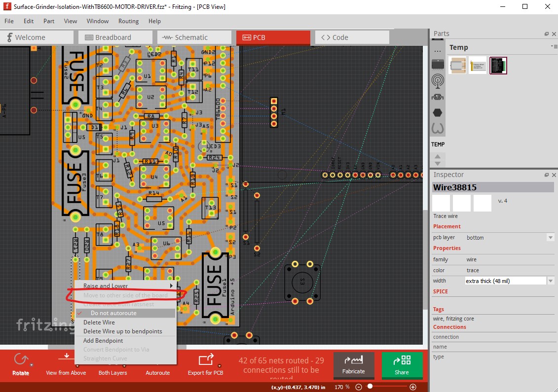
While I’m retired and thus can spend time as pleases me, a lot of this effort is actually chasing the corruption bug (which has been frustrating me for more than 5 years now!) I’m hoping your sketch may shed some light on that. Now I have a copy that routes clean I can compare the corrupted file to a clean one and see it that tells me anything new about the corruption. In this case it may, because the corruption in this case is much worse than any I have seen before. Even if it doesn’t illuminate the original issue it may point to another bug or bugs that we can fix. I’m interested in how and why it managed to change the base operation of Fritzing (changing the color of the traces in pcb.) and if there is anything we can do to prevent that.

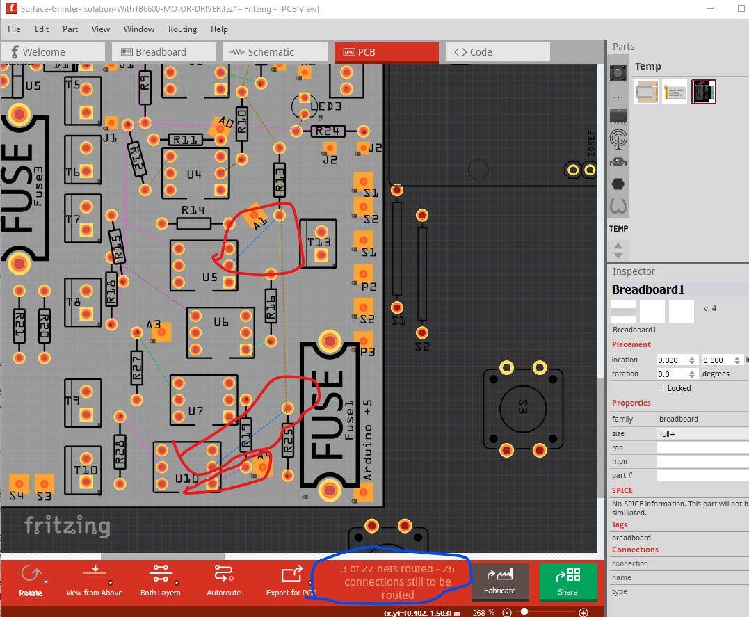
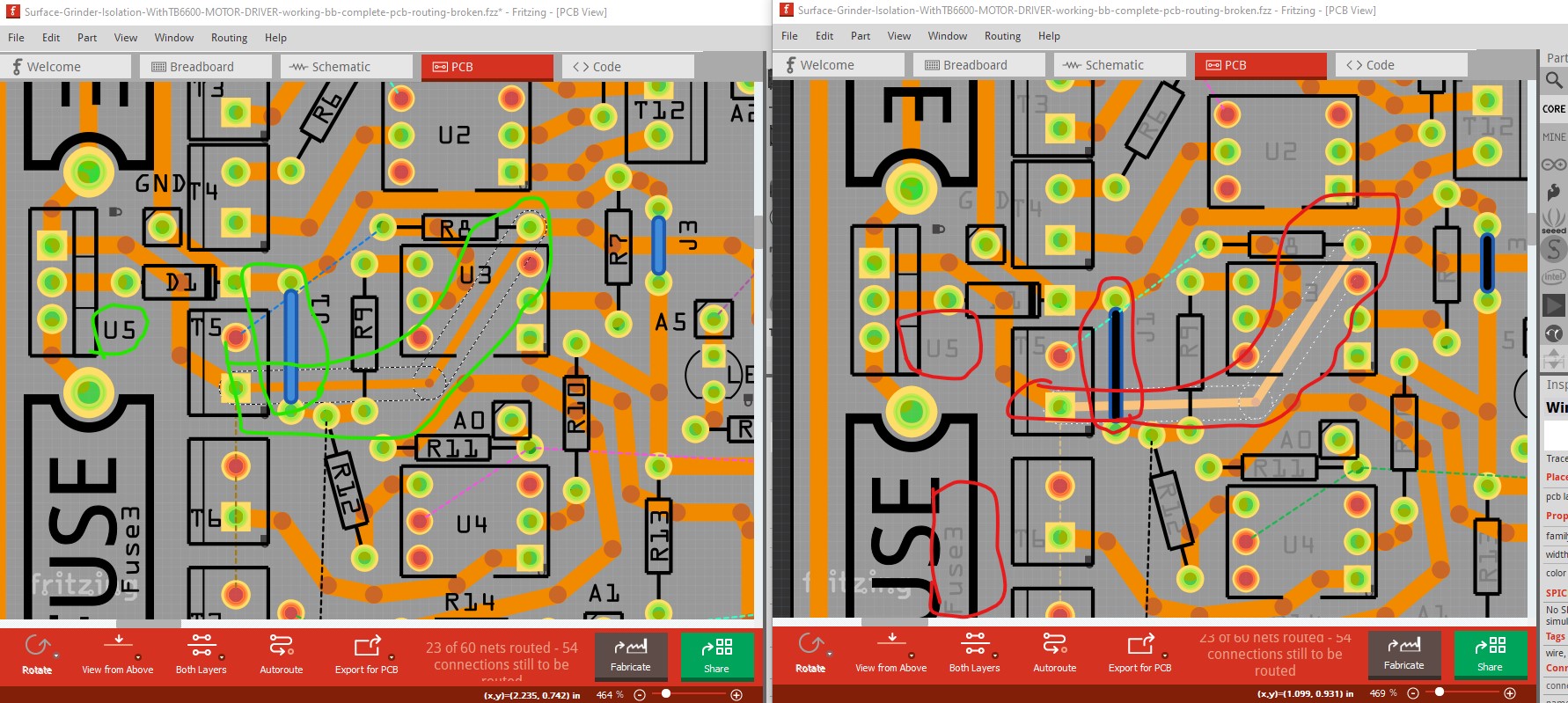
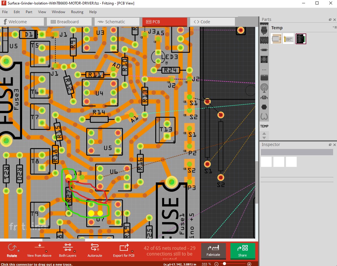
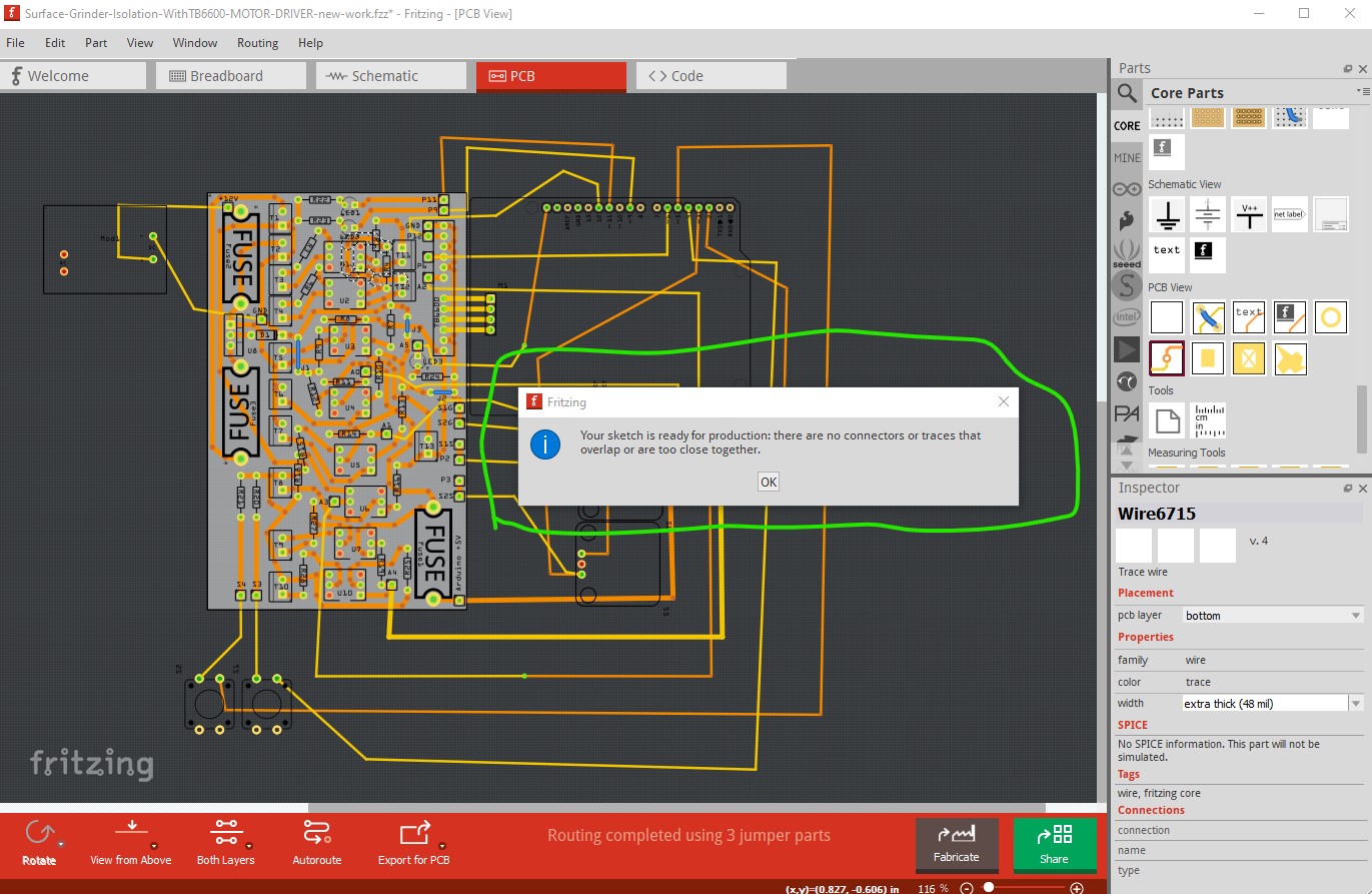
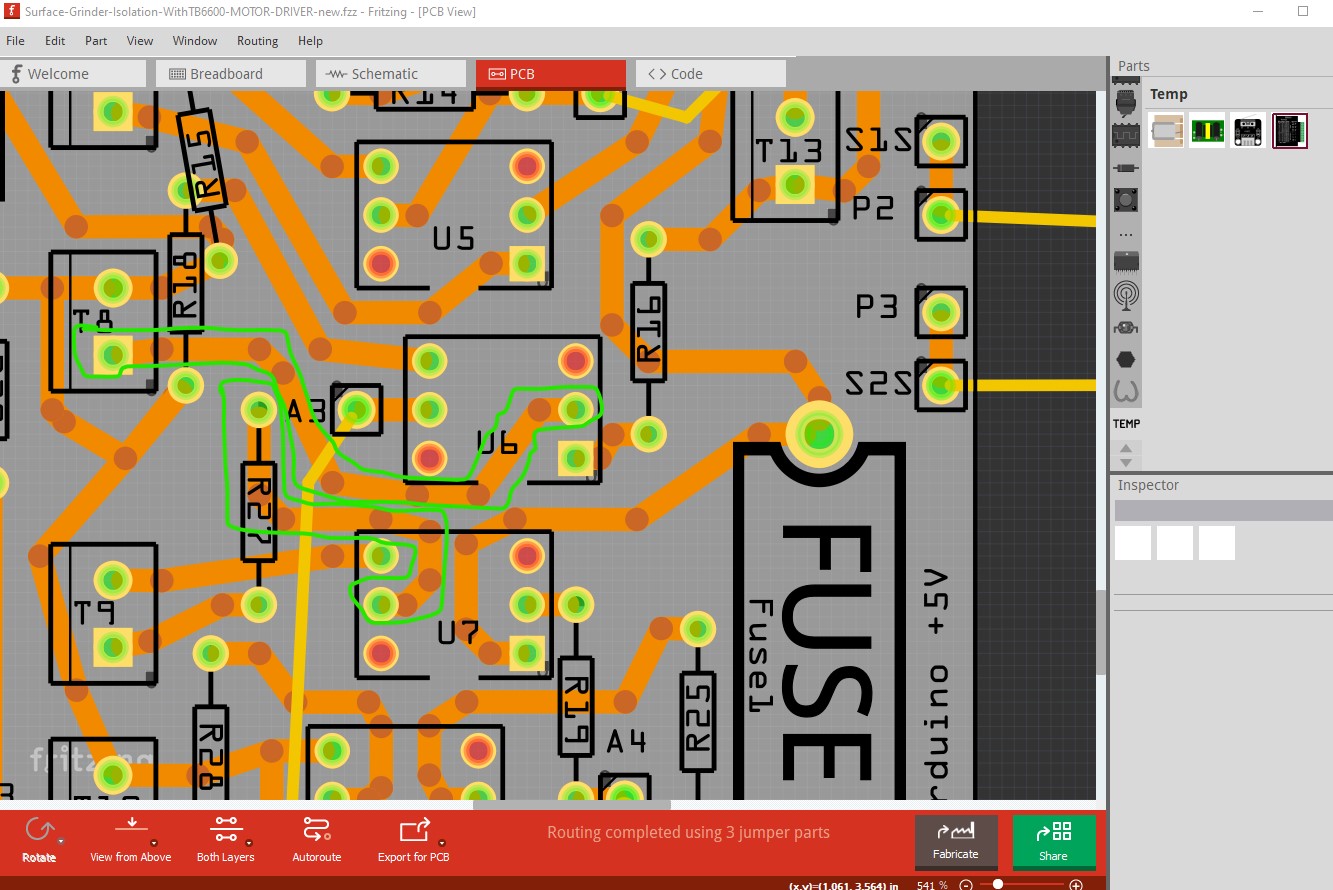
The connections that overlaps aren’t supposed to be connected to each other. Even though they overlap in pcb, Fritzing is remembering they are two different nets (thus the DRC error.) The two nets are separate, but the way they are connected they will short together and make the board not work. My layout (assuming I didn’t make a mistake of some kind) is correct and is routed without the two nets being connected to each other.

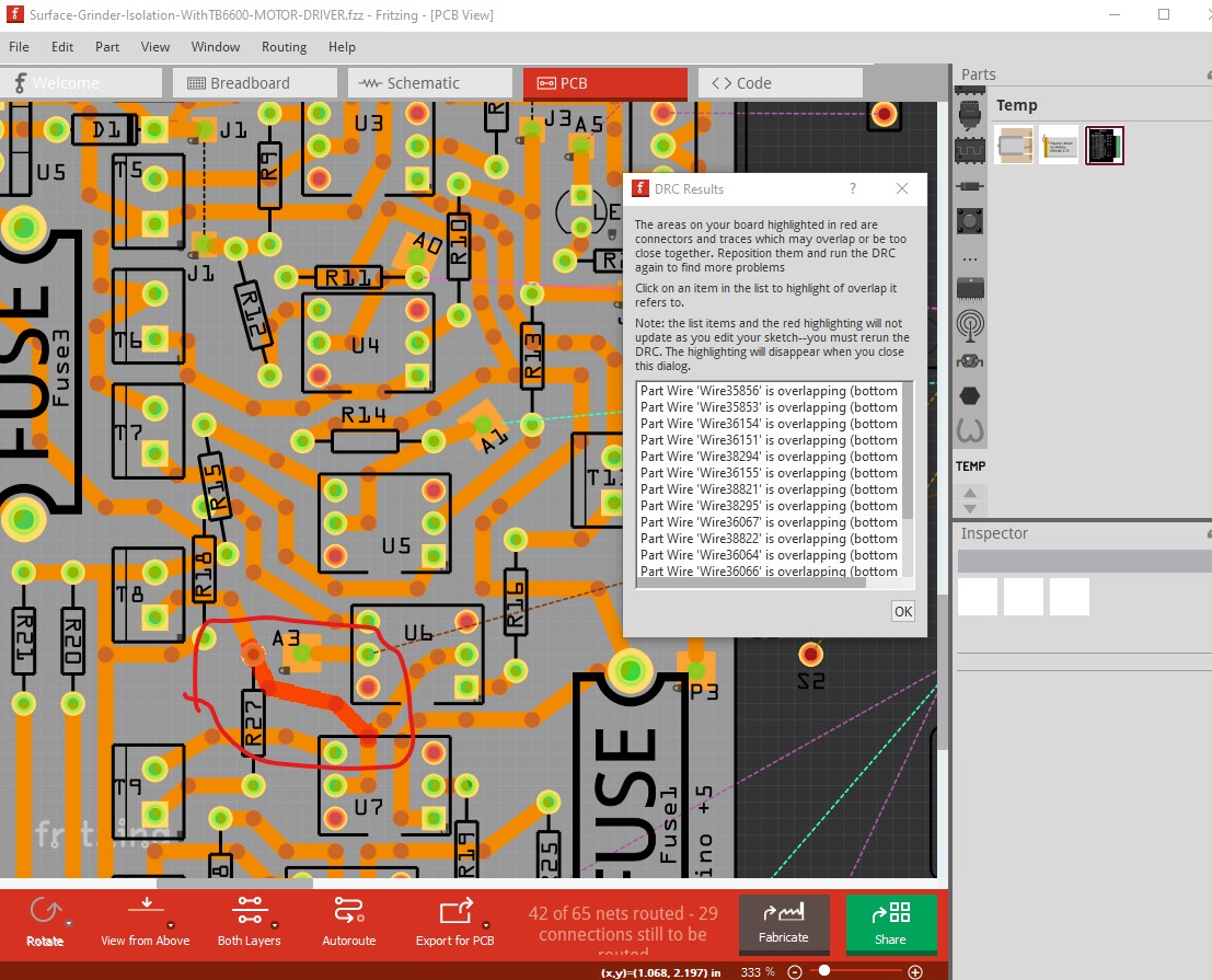
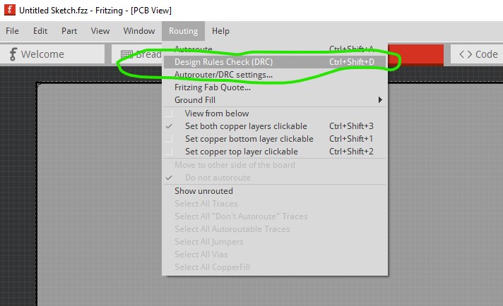
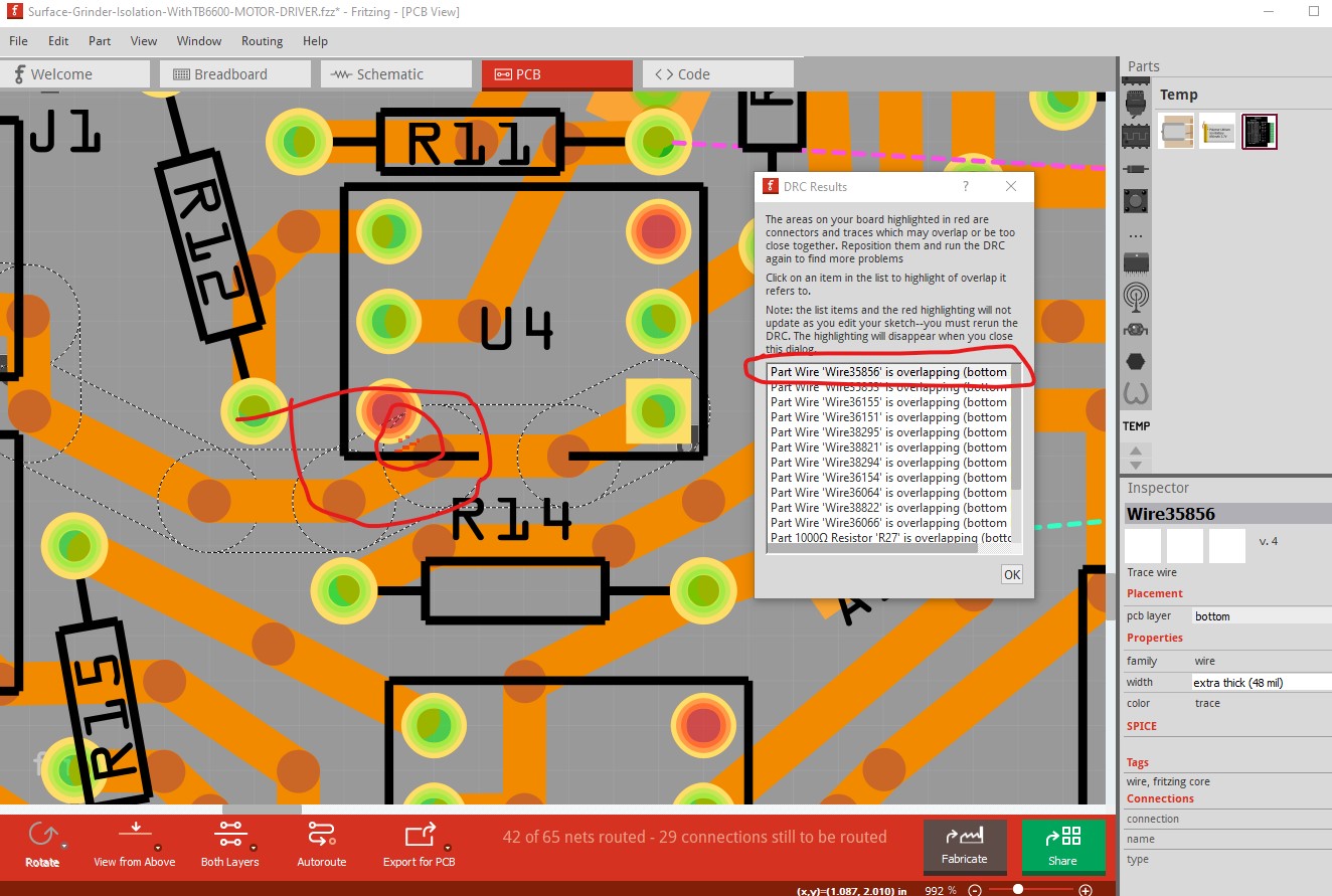
Sorry, I tend to not remember the odder features aren’t obvious to everyone (a danger of using Fritzing for a long time!), DRC stands for Design rules check (Routing->Design rules check)

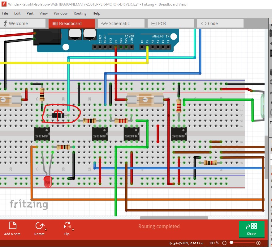
This checks that all traces on the board are far enough away from the edge of the board and from all other traces and parts on the board and (assuming the silkscreen layer in parts are accurate) the parts will physically fit correctly on the board (I notice some of the terminal blocks are pretty close to each other for instance!) so the board should be producible by a board house. The settings line under it can modify the settings for it and autorouter, but by default they are set to professional, which is what is in use here. Clicking an an item in the list highlights the trace in error, then you need to look for the (sometimes painfully small!) red marker that marks the traces that are too close (the trace is the outer red circle and the marker the small red dots in the inner circle in this image.) It is sometimes safe (and necessary!) to ignore warnings but it is good practice to always check for them and make sure they are safe to ignore.

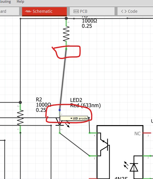
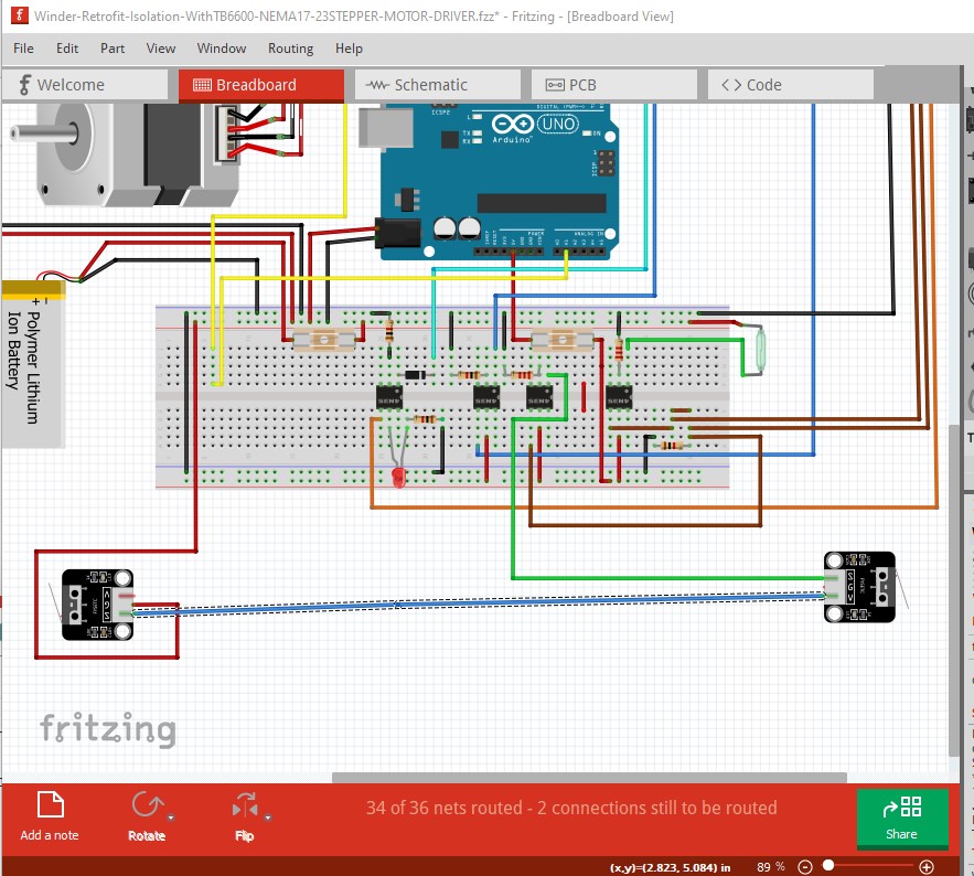
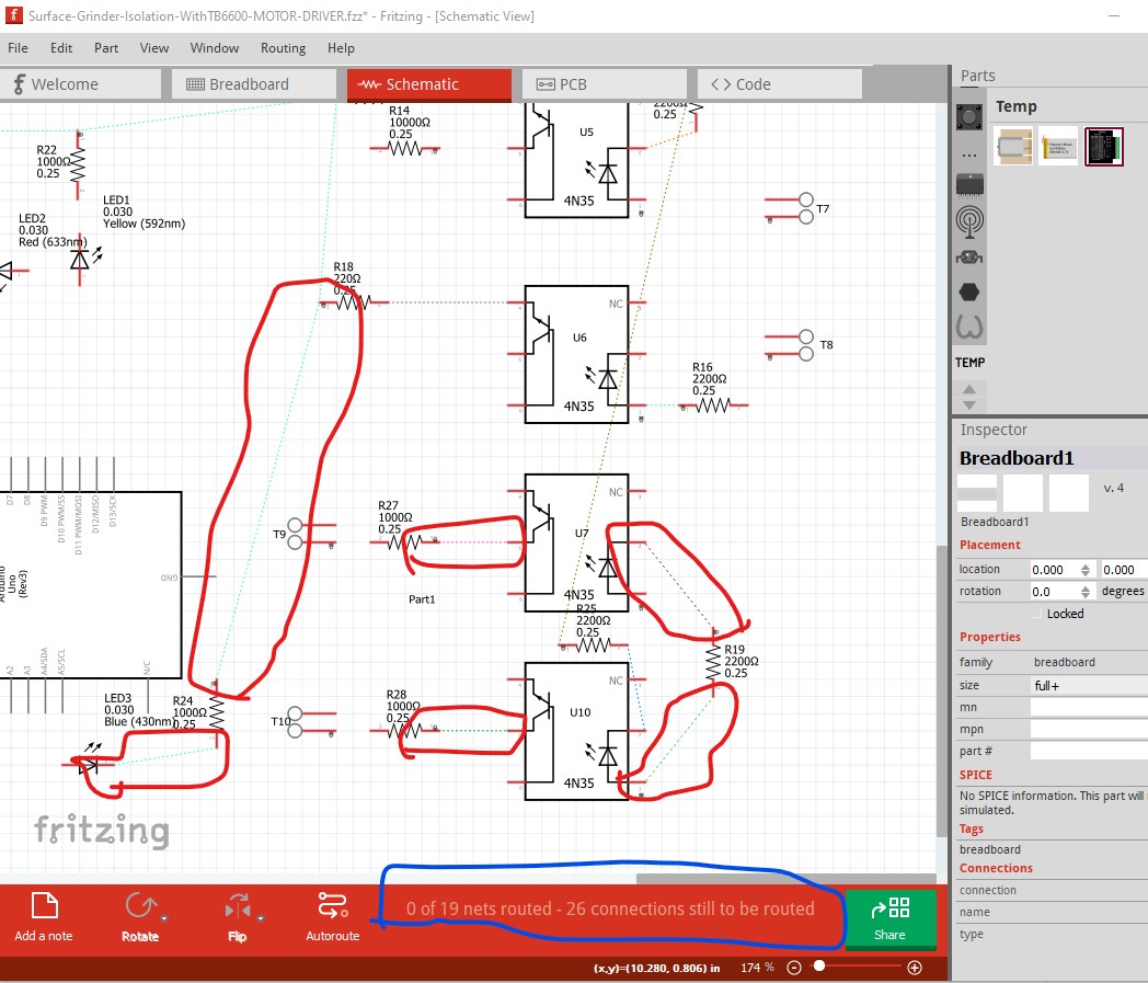
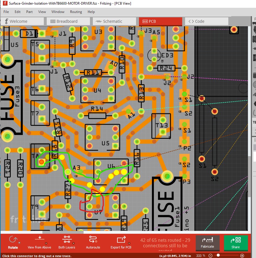
assuming I didn’t screw something up (although I don’t think I did as DRC was complaining) this image of my new routing indicates the problem. In your sketch these two traces overlap and would (because in the end up copper is copper) short together and cause the board to not work because two nets that are supposed to be separate short together.

edit:

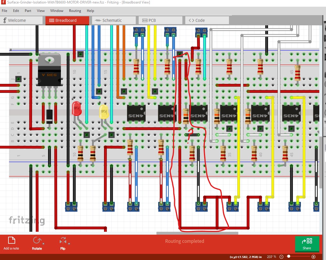
I just came across (or at least just recognized) another oddity:

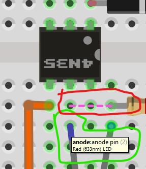
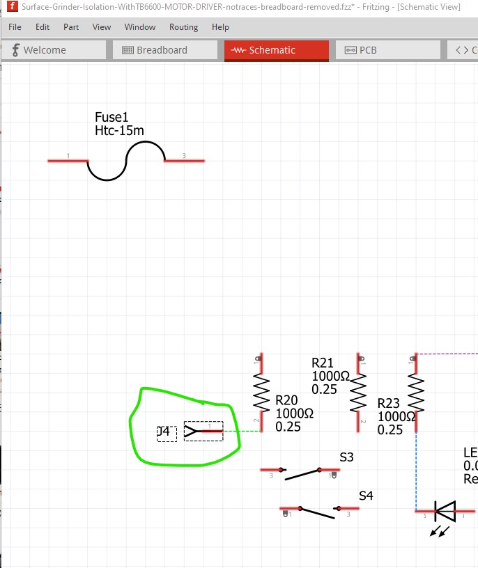
The connection circled in red here seems strange. 12V is going to the terminal block on the red wire, but the black and white striped wire to the optocoupler connects to a 10k pull up resistor to 12V. I would expect the black and white wire to be ground or at least pull to ground to activate the optocoupler but then I would expect the 12V connection to the terminal block to connect to ground instead to supply whatever is on the end of the terminal block with the necessary ground. It is probably worth looking at this connection to make sure it is correct (I can’t tell since I don’t know what is in the end of T5 or T13 so it may be fine as is!)

edit1:

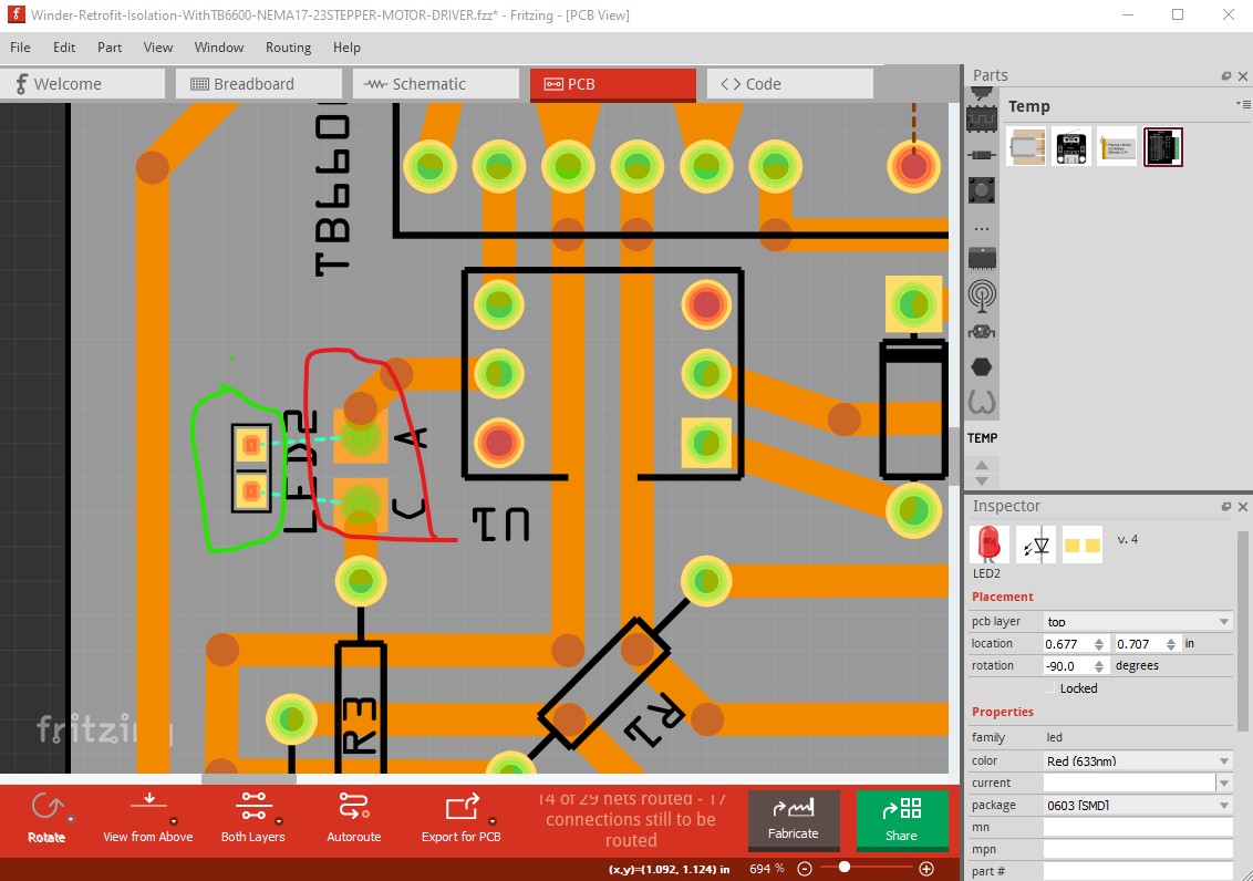
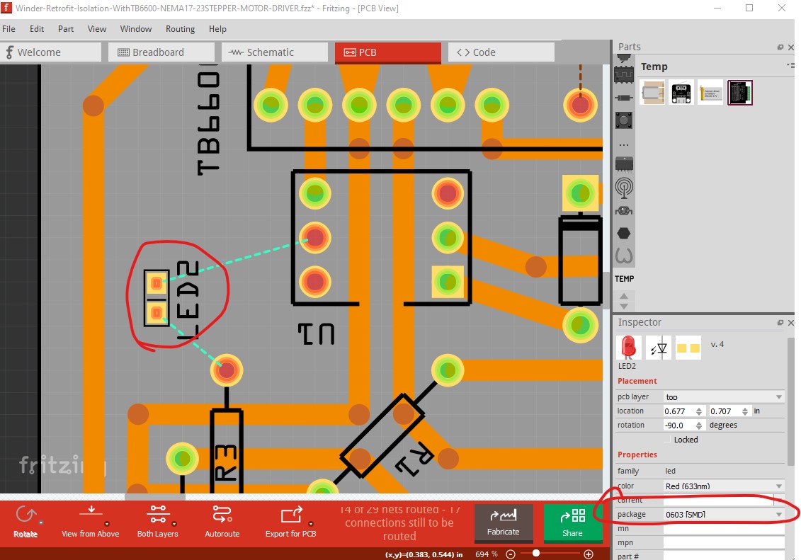
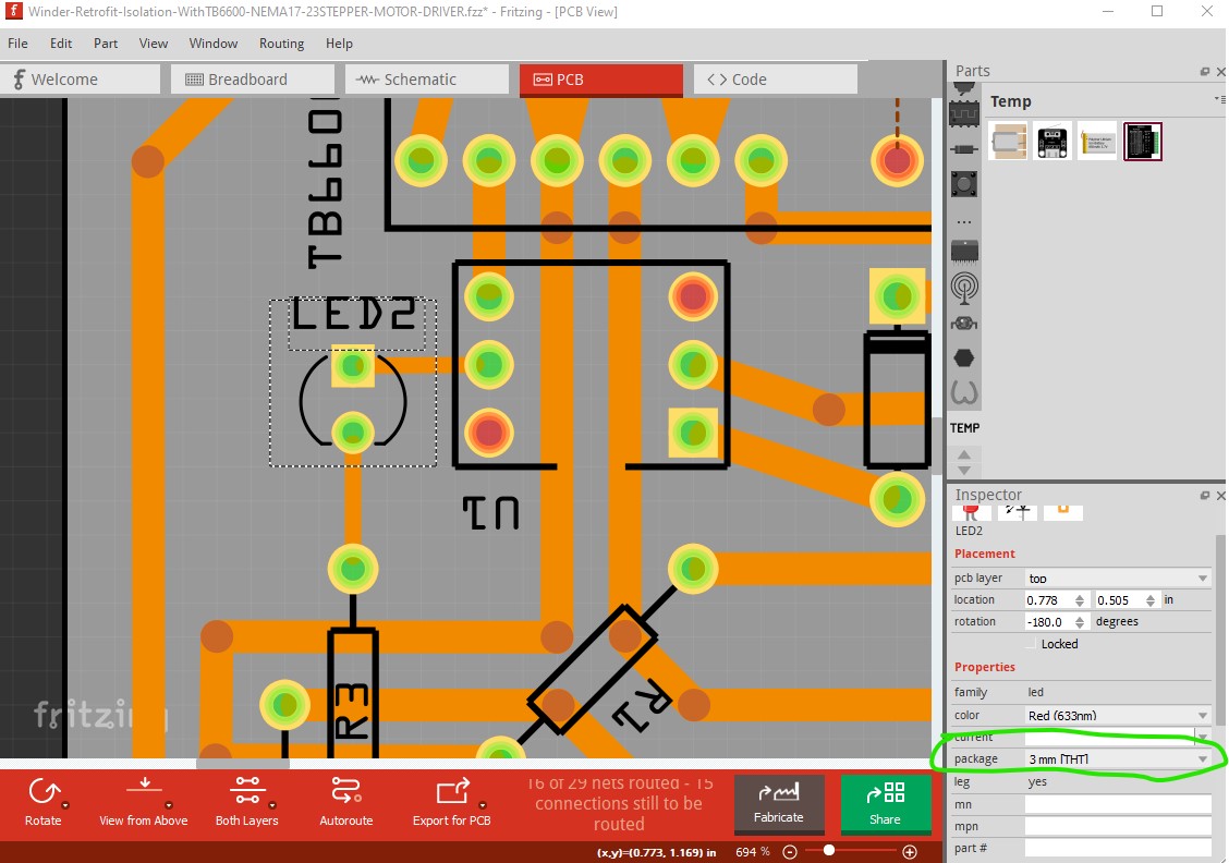
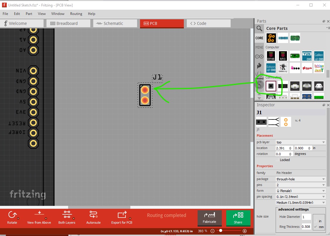
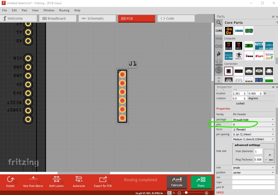
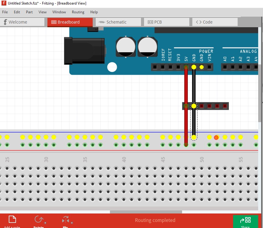
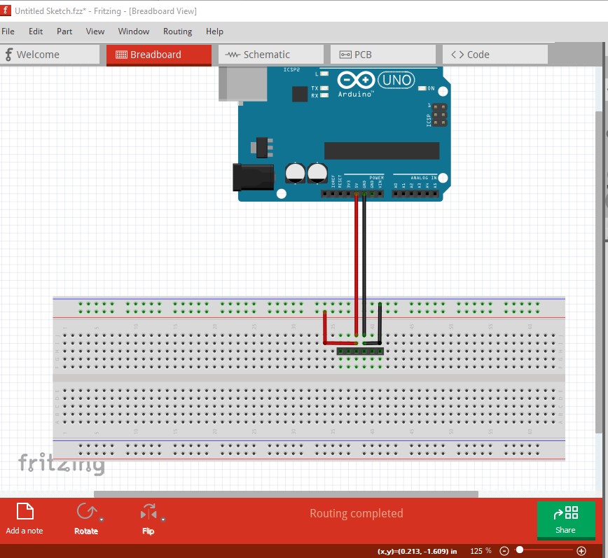
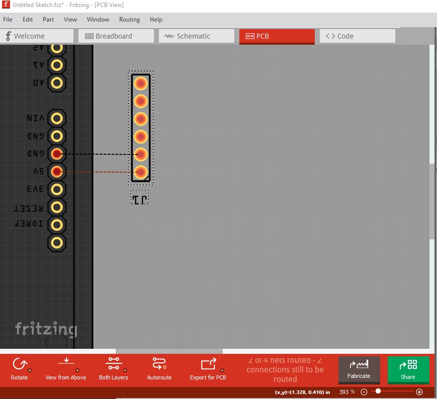
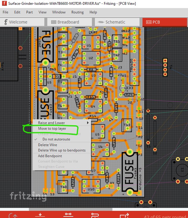
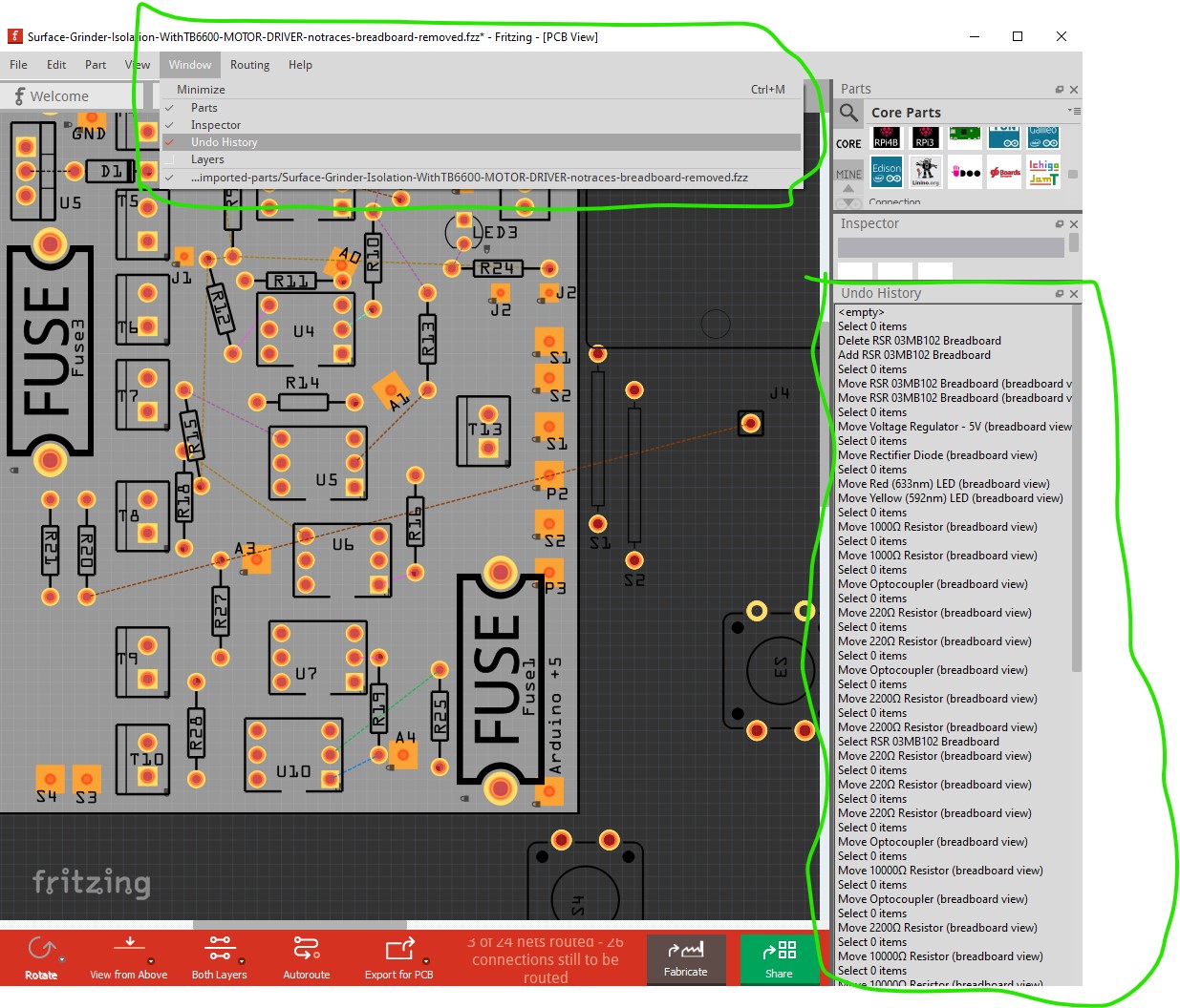
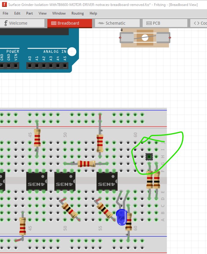
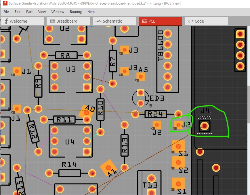
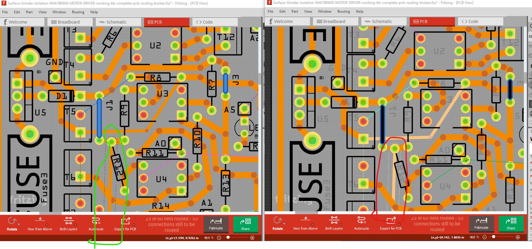
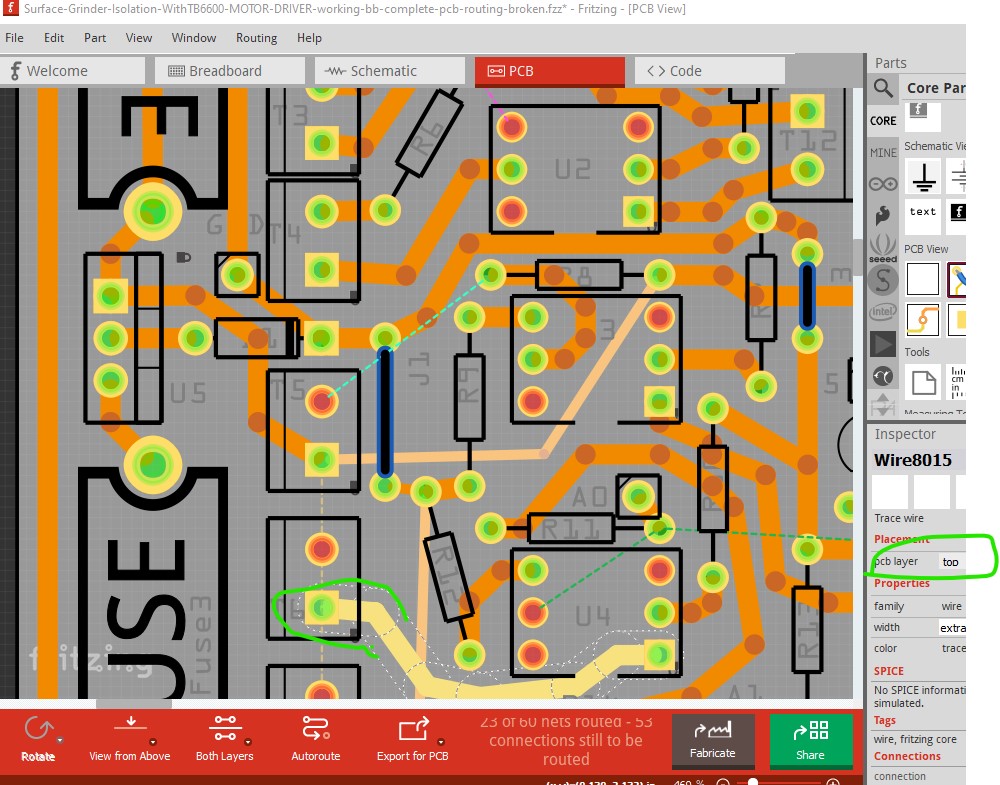
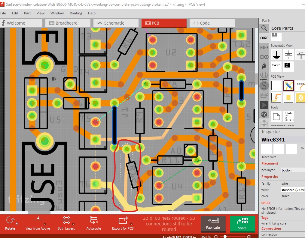
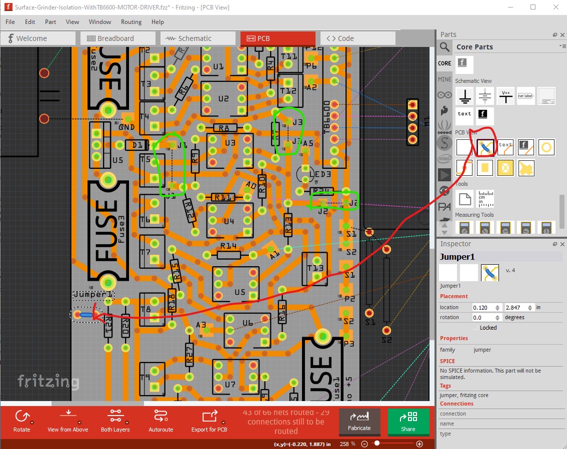
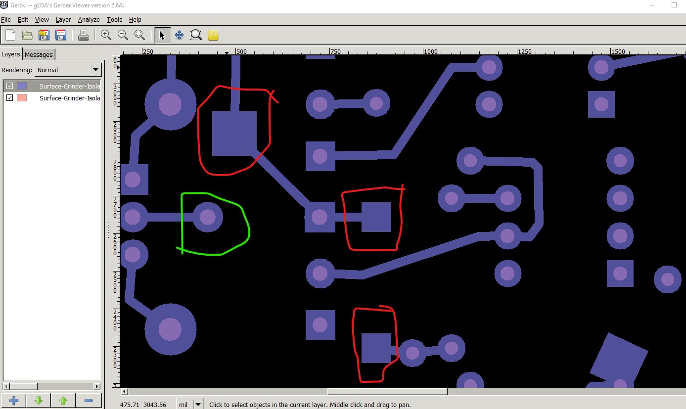
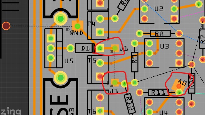
I just figured out the cause of our problems. It isn’t database corruption at all, but rather your choice of pads. The pad you used is only on one side of the board either top layer or in this case bottom layer, but they are SMD type pads and thus despite looking like they have a hole in Fritzing in the gerber output they do not. Because they are only on the bottom layer the trace can not be moved to top layer (because there isn’t a through hole connection because the pad is single layer.) It looks like there is another bug somewhere which caused the color change I saw on the original sketch (I so far haven’t been able to reproduce that one!) The reason my new sketch works is because the headers I used as the pads are through hole and will both let me change layers and drills a hole in the gerber output. Here is a screen shot of the pcb view with some of your pads from Fritzing. While the green dot (which appears to represent the connection point, not a hole!) looks like a hole should be produced it is in fact not. The fact the pad is only showing on the bottom layer (as it is brown not golden like the through hole pads) should have alerted me to what was wrong, but it didn’t until just now.

capture

although it appears to have a hole in pcb view the gerber output has no hole because there isn’t a circle in the pad (and it isn’t through hole) to create one. This is the gerber output (displayed by gerbv) for the copper0 and drill layers in the gerber files.

Note a through hole pad (circled in green here) has a hole. The ground and 2 j1 pads (and the A0 pad on the left edge) do not have holes and I expect they won’t get drilled when you mill the board because the holes aren’t in the gerber drill file. The solution is to use the through hole headers as off board connect points as I did in my sketch. That should do what you want. This is another Fritzing quirk, gerber processing takes place after the render for pcb view and will sometimes (as in this case) show holes in pcb view where in fact the hole isn’t in the gerber file (which is why you should always check the gerber output with a gerber viewer before ordering boards!) At this point I don’t think your original sketch had database corruption (I can’t find any evidence of it) just this quirk of how Fritzing works which took some time for me to figure out.

Peter

I will have to look at U3 a bit more carefully, at the moment it is a SPARE.

U1 & U2 are remote equipment interfaces. U3 was to be a different remote interface.
I may have to remove one of the resistors from that circuit.
Your discovery of the PADs not being THROUGH hole explains why I had to add holes
to the LIGHTBURN model from the FLATCAM SVG. There were more than a dozen holes
missing as I prepared for a “TEST BURN” of my board layout from Flatcam’s output.
( but easy to repair in LightBurn ) so I just thought it was a glitch in Flatcam. I will get rid of
those pads in the next model for sure.
Thanks a heap for your analysis, I too am retired for more than 10 years now,
with more projects now than I can ever complete in my lifetime…PLUS all of the
HONEY-DOs I encounter daily.
The PC Boards I etched ( OUTLINE TRACING ) appeared quite good, I just have to
drink a couple beers to steady my hands before soldering the components to them
due to the close proximity of traces to adjacent copper in this type of board.
( less than .5mm between ) Lots of folks are CNC fabricating this type of
board for their projects. I fabricated a couple “Traditional Trace” smaller boards last week
that came out perfect, but opted to use the outline method on these larger boards
to prevent overexposure at the edge of traces from the laser on this larger board.
Thanks,
Bill