Confused about New Part Fab

My other problem with all this is warningsā€¦earlier I screwed up and deleted files I had to recoverā€¦
Other Problem

The svgs uploaded just fine. If you right click on the image and select ā€œsave file asā€ it will download as a svg.

That said the svg is consistent with the images above, a grey square (the white square which is the view box in the svg) with the connectors because that is all that is in the svg. The original part breadboard svg looks like this:

svg.breadboard.prefix0000_911c140c21fa07989d9ddccd6943645a_1_breadboard

and like this in Inkscape

your svg only has the connectors not the rest of the image. It looks to me like you imported an image of the actual part (which isnā€™t that desirable as it isnā€™t a vector image and wonā€™t scale) it is preferred to make the image out of drawing elements (although it is a lot more work!) as in the original svg. You also need a group which contains the entire svg with the label breadboard to make sure you part will export as an image. I often start from an imported image like this and over lay the image with svg elements then delete the image. I would probably start with this breadboard svg, rotate it 90 degrees to match the orientation of yours and replace the generic screw connectors I used with an outline that matches the one in your image (moving the connectors over the screws in the terminal block) as being the easiest. First select the breadboard group and rotate it 90 degrees:

Then ungroup it for easier manipulation and import the jpg image of your screen above and rescale it to be the same size as the current part (you actually want it to be the same size as the real part!)

Here I moved the image over the part then selected the black rectangle and moved it above the image so the text is overlaying the image making it easier to move around.

then move and change the text as needed to make it match the image. Here I changed the text from all upper to upper and lower then adjusted the font size til the text matches.

now you need to do the same or all the rest. Then you need to create a part for the terminal blocks (because I donā€™t have one to copy!) like this from rectangles and circles for the connectors. Start with a rectangle

then move it over where it should be and duplicate it for the next section make it darker green and place it.

Now move both the rectangles back so they are out of the way like this then duplicate the right rectangle (so it is the same color) and resize it to be one of the bars like this

duplicate and resize a bar and make it darker then duplicate them down the row

Then make a circle for the pin (although this isnā€™t the connector as it has a stroke and fill set!)

Now move back to the bottom circle, duplicate it (to make the connector) set fill and stroke to none and set the id to connector0pin like this

rinse and repeat for the rest of the connectors in order.
Then delete the image and move the rectangles until they donā€™t over lap to get the final product with the connectors set.

Finally do an Edit->select all, Edit-> resize page to selection, Object->group and name the resulting group breadboard to create the final svg (this one isnā€™t complete though!) then File->save as and select type plain svg and save the svg. Here is a copy of the svg above so you can see what I did.

svg.breadboard.breadboard_1_breadboard

Hope this helps, if not feel free to ask!

Peter

This indicates you have two parts with moduleId TB6560_V2-DF_1. To fix it you need to change the moduleId on one part or the other. Editing C:/Users/Bill/Documents/Fritzing/parts/user/TB6560_V2-DF_1.fzp and changing this line

module moduleId=ā€œfc-51ā€ referenceFile=ā€œfc-51.fzpā€ fritzingVersion=ā€œ0.9.10ā€

from ā€œTB6560_V2-DF_1ā€ to ā€œTB6560_V2-DF_2ā€ (assuming the moduleId is TB6560_V2-DF_1!) should fix that. You may also need to change the svg files if they are identical to the other part i.e. you may need to change the file name fc-51_breadboard.svg below to something unique such as fc-51_2_breadboard.svg (where there isnā€™t an svg file named that in Fritzing.) You then also need to change the svg file names to match those set in the fzp file. The svg files will be in /Bill/Documents/Fritzing/parts/svg/user/breadboard (and icon, schematic and pcb)
Presumably you have two fzpz files that have TB6560_V2-DF_1 with the same or different svg files. The modulerId and (usually) svg files need to be unique.

<iconView>
  <layers image="breadboard/fc-51_breadboard.svg">
    <layer layerId="icon"/>
  </layers>
</iconView>
<breadboardView>
  <layers image="breadboard/fc-51_breadboard.svg">
    <layer layerId="breadboard"/>
  </layers>
</breadboardView>
<schematicView>
  <layers image="schematic/fc-51_schematic.svg">
    <layer layerId="schematic"/>
  </layers>
</schematicView>
<pcbView>
  <layers image="pcb/fc-51_pcb.svg">
    <layer layerId="silkscreen"/>
    <layer layerId="copper0"/>
    <layer layerId="copper1"/>
  </layers>
</pcbView>

Peter

Peter,
Thanks for the help. I havenā€™t addressed the last problem yet, but upon receiving your reply last night, I realized that IMAGES donā€™t work. I have several lasers that are run with LIGHTBURN, and I commonly TRACE images with it so I TRACED my downloaded image and re-fabricated the SVG in LIGHTBURN with THEIR CAD capabilities, and simply exported the svg. Simple, extremely quiick, and accurate. You can use a 30 day version for free ā€¦ other Fritzing users might want to give it a try. I converted all text to PATH before export from LIGHTBURN to prevent font discrepancies. I need to find out how to scale the part about twice the displayed sizeā€¦ the SVG was scaled to component size, then increased in Inkscape, but has remained the same size.
Additionally my FILE OPEN window went to FULLSCREEN and I cannot reduce itā€™s size.
I believe this part is pretty much ready for public releaseā€¦It seems to do everything I wanted, and I know there were several other requests for it.
Thanks a lot, Bill
BreadboardWithTB6600-NEMA17-23STEPPER-MOTOR-DRIVER.fzz (122.2 KB)
BreadboardWithTB6600VER4.fzz (107.3 KB)
SCHEMATIC-TB6600
TB6600-LBRN-FAB
Updated-Stepper-Driver03-TB6600

By the way, I am using the exports from PC Board fabrications from Fritzing to "Burn" small Printed circuit boards using POSITIVE ACTING Pre sensitized PC board, then through LIGHTBURN to my lasers. The trick is SPEED and extremely low power. Outline, Trace, and Solid can all be done with a lot of trial and error this way.

Bill
Isolated-NPN-PNP-Pair-2.fzz (19.1 KB)

A few problems in your part. Here is the output (only the errors not the warnings :slight_smile: ) from your part:

Error 69: File
ā€˜svg.breadboard.TB6600-UPDATED-STEPPER-DRIVER-04_461729d0ec852d1a76305f3c4a7c45aa_9_breadboard.svg.bakā€™
At line 25

Found a drawing element before a layerId (or no layerId)

Error 69: File
ā€˜svg.schematic.TB6600-UPDATED-STEPPER-DRIVER-04_461729d0ec852d1a76305f3c4a7c45aa_9_schematic.svg.bakā€™
At line 13

Found a drawing element before a layerId (or no layerId)

both breadboard and schematic lack layerIds which will cause the part to not export as an image.

Error 18: File
ā€˜part.TB6600-UPDATED-STEPPER-DRIVER-04_cfc8dd5449c9306d0950c3358bf53b84_3.fzp.bakā€™

Connector connector1terminal is in the fzp file but not the svg file. (typo?)

svg svg.schematic.TB6600-UPDATED-STEPPER-DRIVER-04_461729d0ec852d1a76305f3c4a7c45aa_9_schematic.svg.bak

indicates the schematic has not terminalIds (normally a problem, but not in this case due to an odd schematic layout.)

Connector connector2pin is in the fzp file but not the svg file. (typo?)

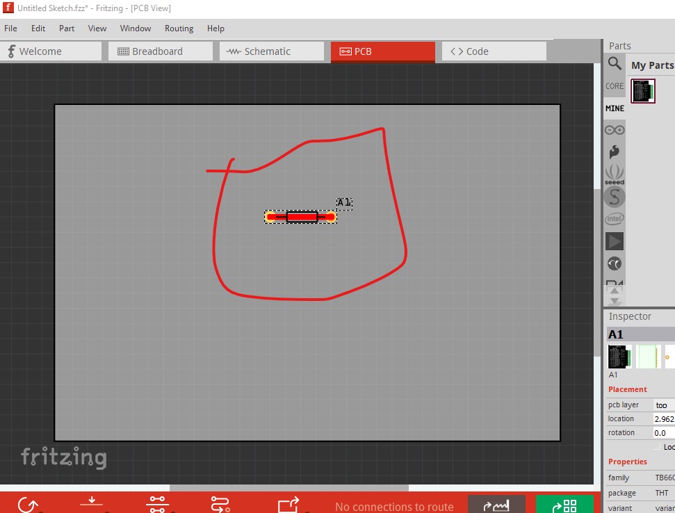
svg svg.pcb.TB6600-UPDATED-STEPPER-DRIVER-04_461729d0ec852d1a76305f3c4a7c45aa_9_pcb.svg.bak

which causes this in pcb view (as there are undefined connectors)

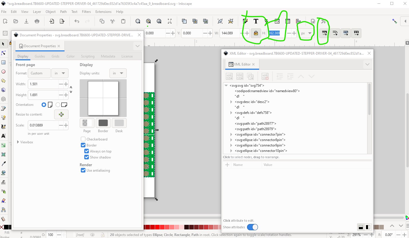
So lets start with breadboard.

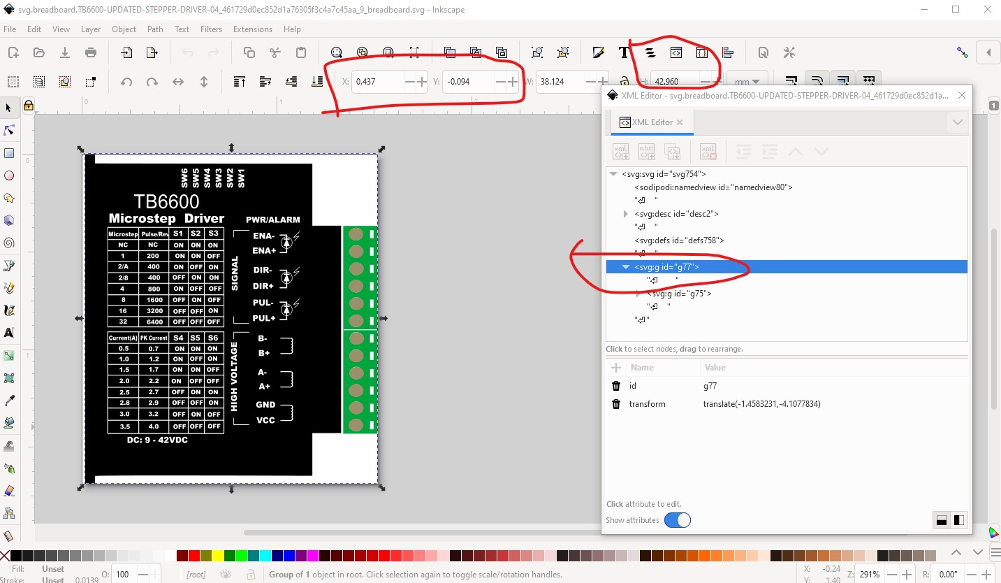
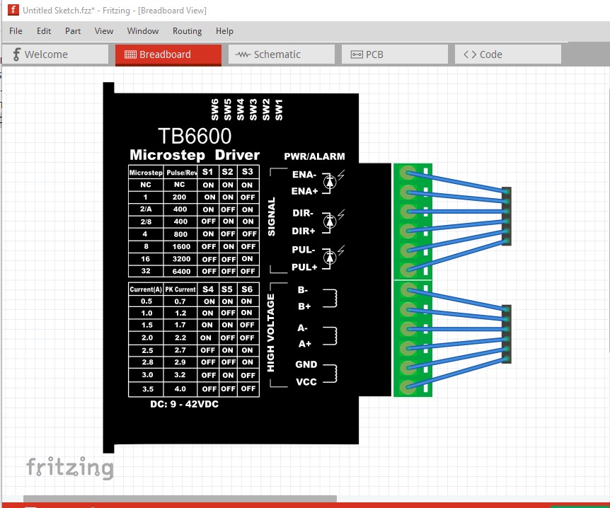
the group circled in red needs to be changed to breadboard so breadboard would have a layerId. The x and y should start at 0 (not doing so can cause offsets from the grids) and as you note the size of the part is about 1/2 to small (49mm against 96mm)

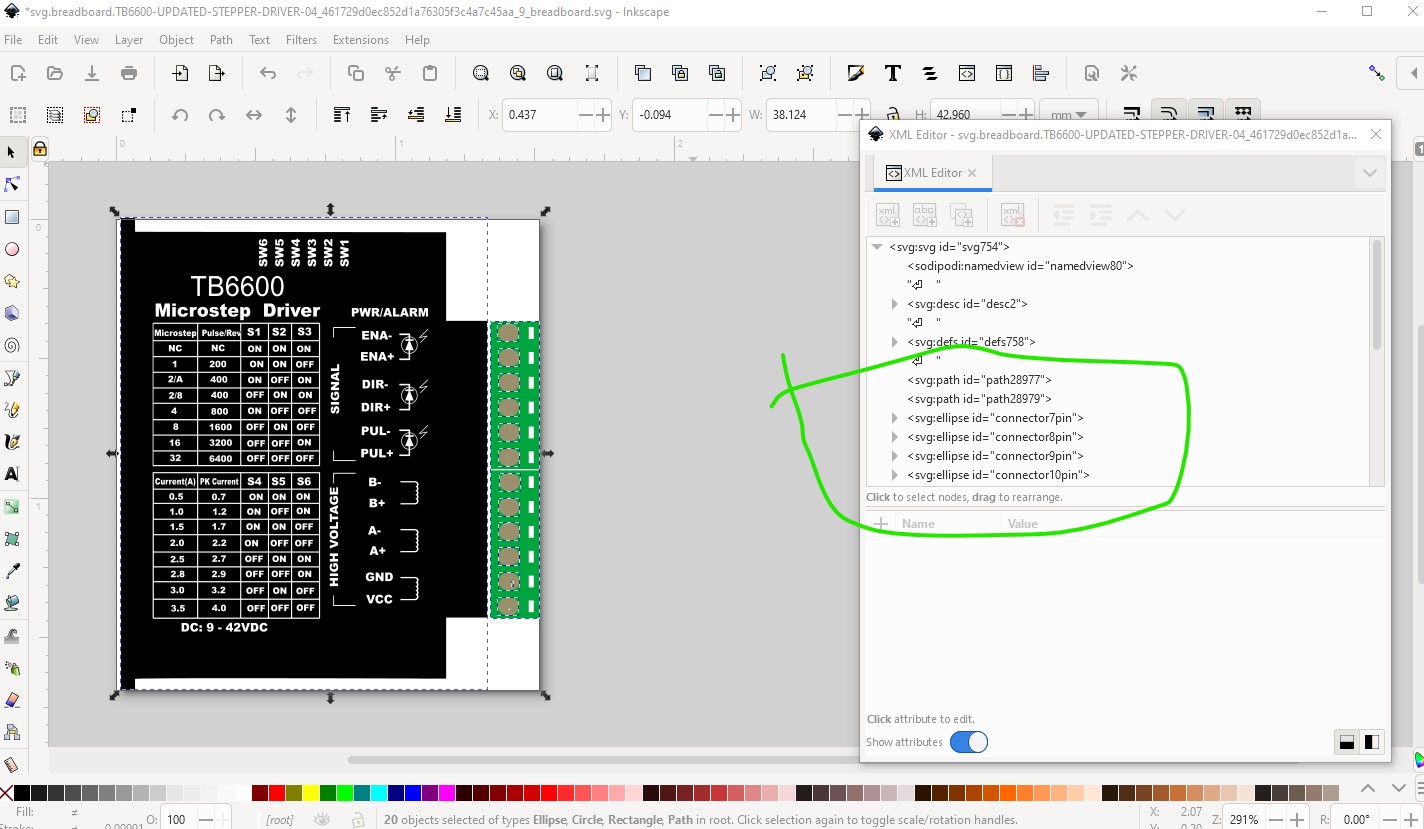
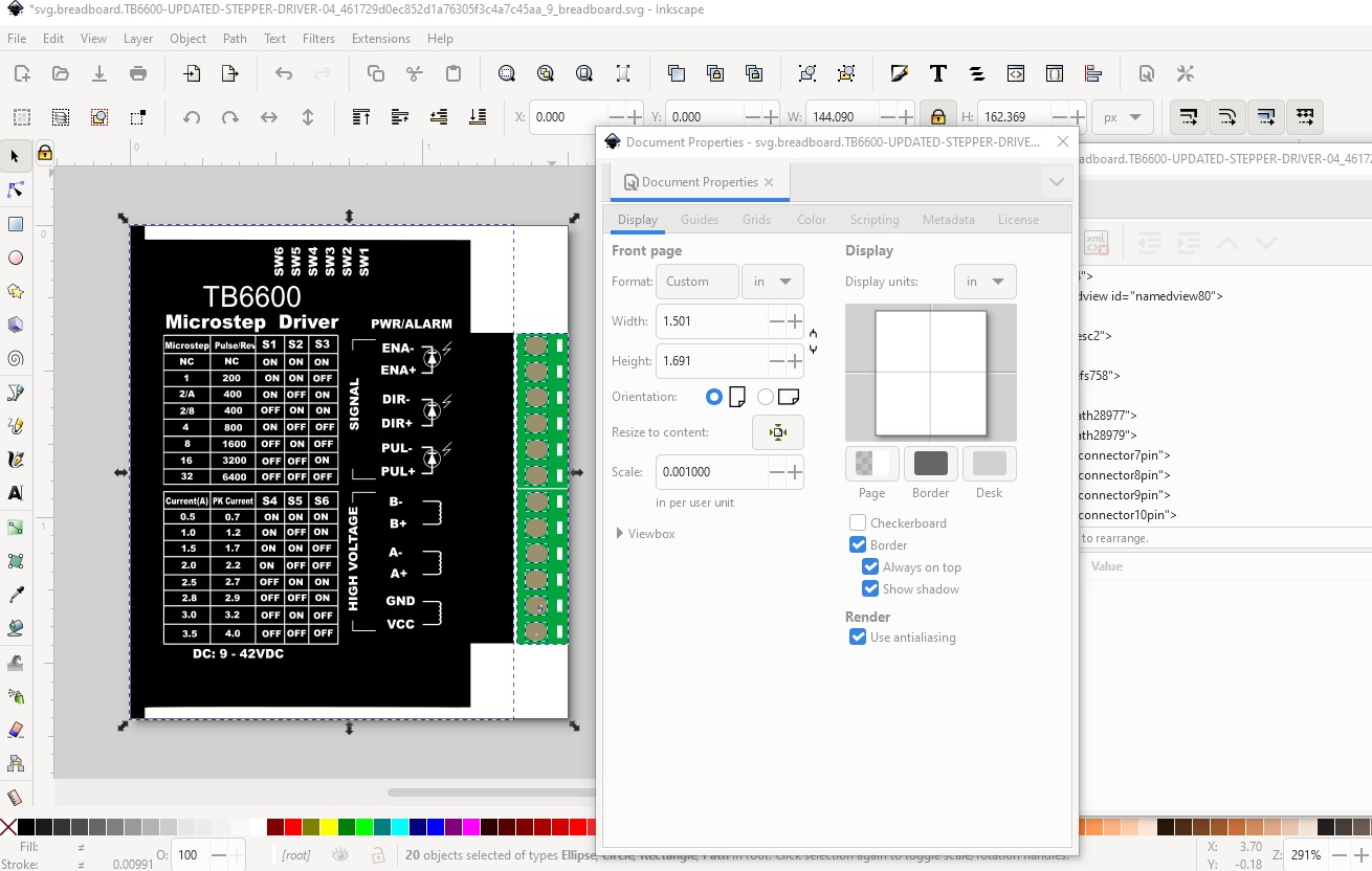
so first I ungrouped the entire svg which is a requirement for successful scaling in Inkscape by selecting the top group and hitting cntrl-shift-g multiple times til there are no groups left.

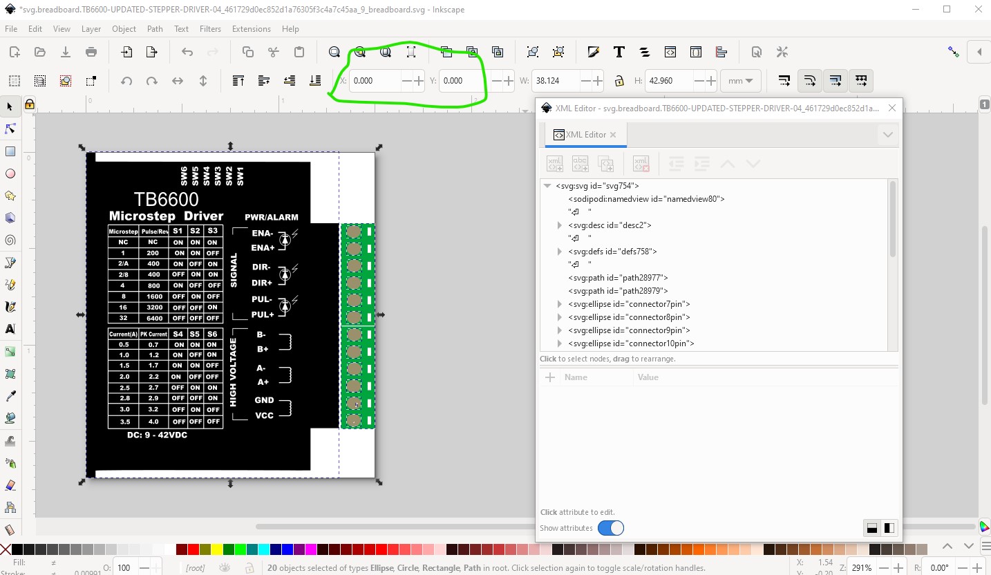
then clicked Edit->select all then Edit->resize page to selection to reset the view box to 0 0

then I corrected the scale of the svg. In Fritzing it is desirable that the viewbox set drawing units at 1/1000 of an inch (which is a scale of 0.001 in the red circle here.) To correct this

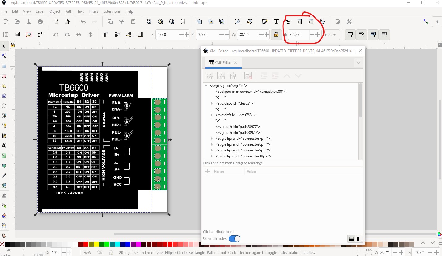
lock the width to height, change the dimensions to px (for maximum resolution) and copy the larger of height or width (height in this case) to the clip board (or record it somewhere) then change the scale from 0.013889 to 0.001 which will make the image much smaller. Then set the height back to the same value it had before the rescale like this

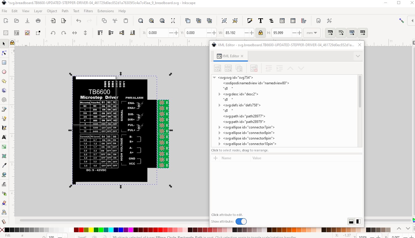
now we can change back to mm and change the height from 43.960 t0 96 to be around the correct scale (it isnā€™t clear to me where that 96mm ends, at the end of the terminal strip as I assumed or at the edge of the case, so it may be wrong!)

now we are again outside the view box,

so Edit->select all and Editā€“>resize page to selection to correct that.

now to renumber the pins. Convention in Fritzing is that connectors should start at 0 and increase linearly with connector0 being at pin1 of an IC (so on the lower left) here that translates to the right bottom

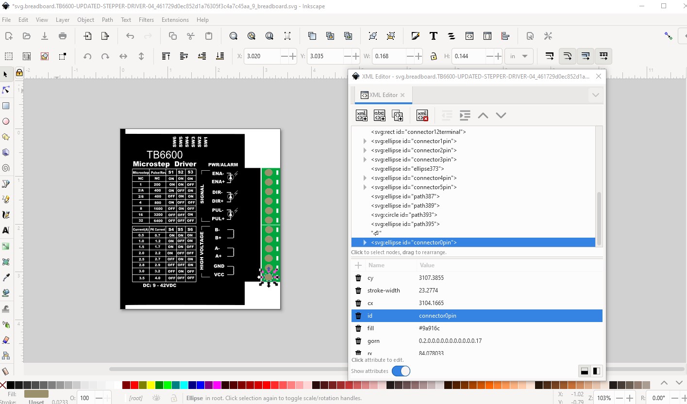
I prefer to move all the connectors to the bottom of the svg because I have a script that will renumber them automatically (although it broke in this case because of the title elements on the pins!) So now move and renumber the connectors like this (connector0 here started out as pin6)

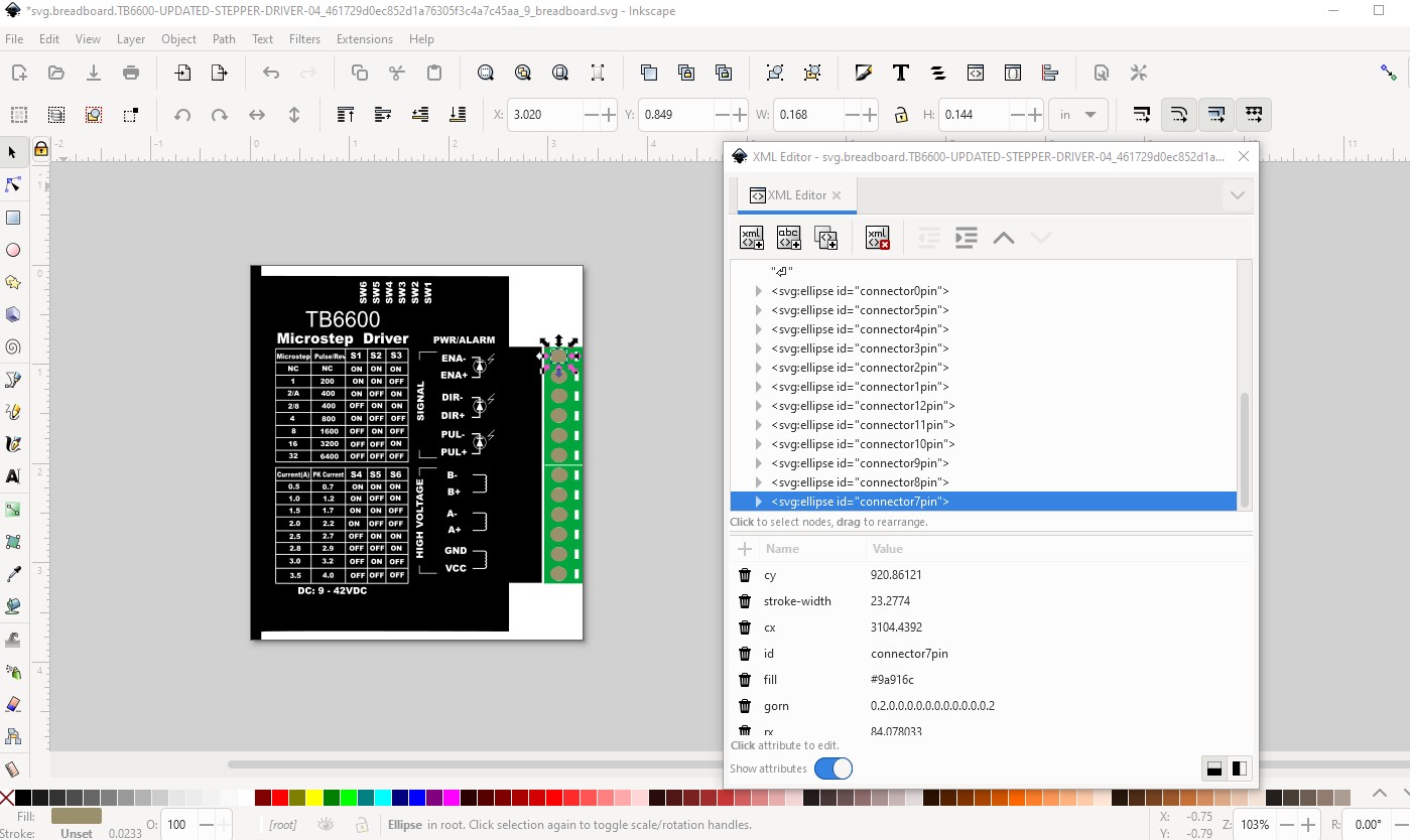
ending up looking like this

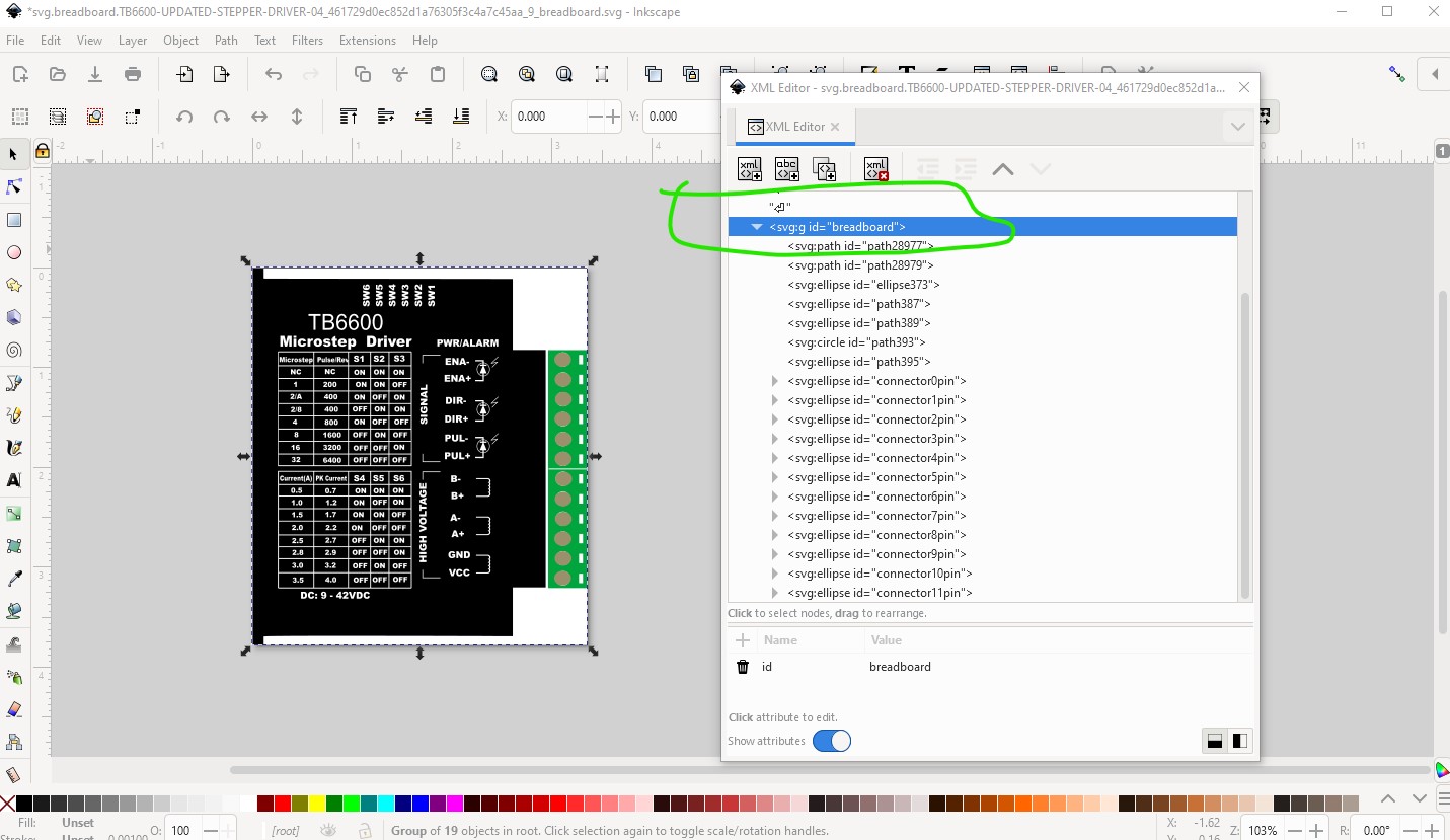
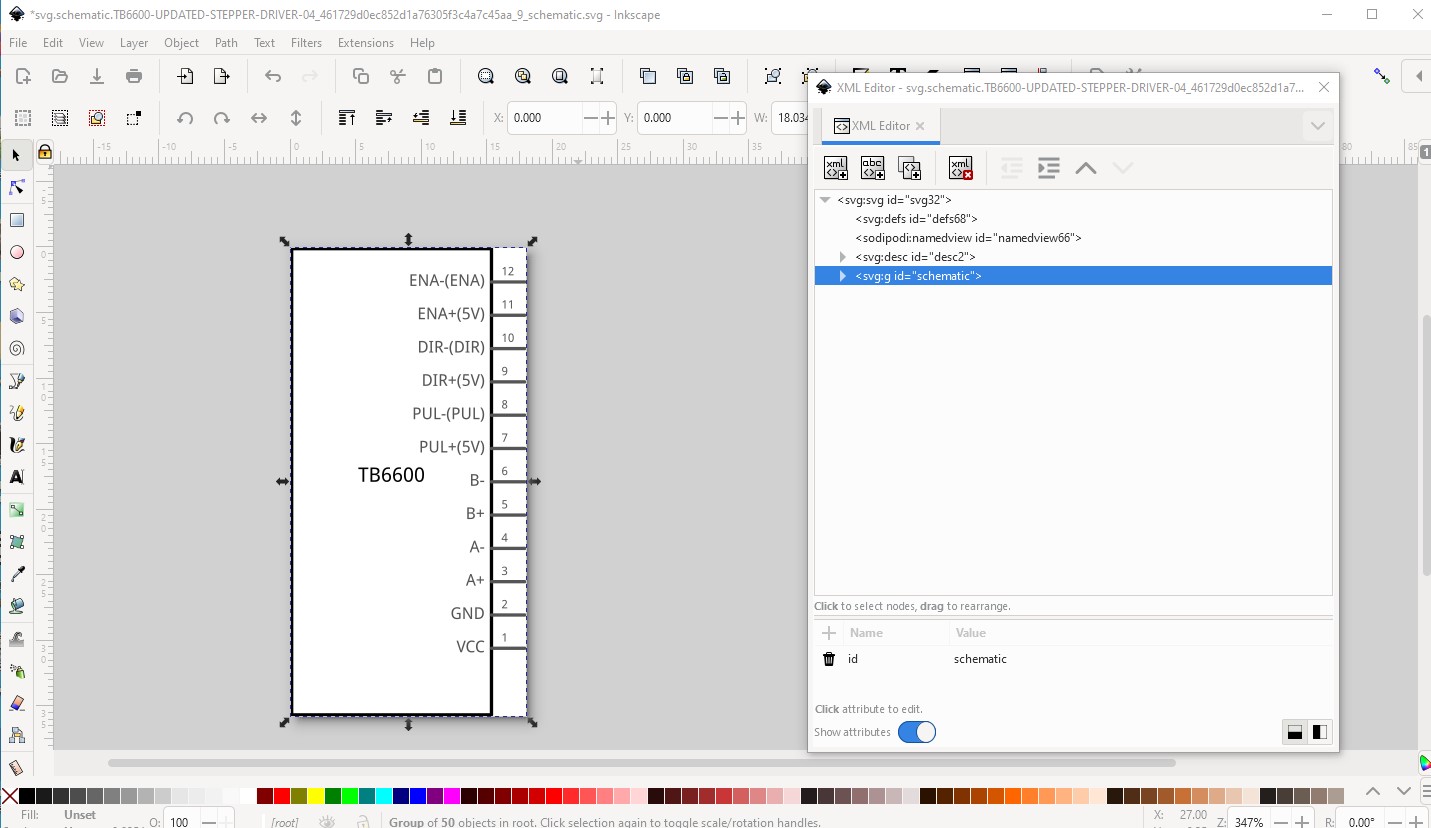
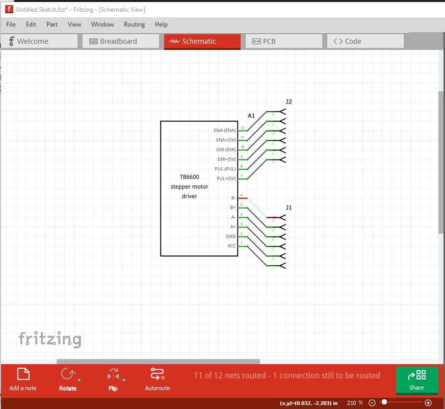
then Edit->select all, Edit->resize page to selection, and Object group and rename the created group breadboard to create the correct layerId. From there on to schematic which currently looks like this
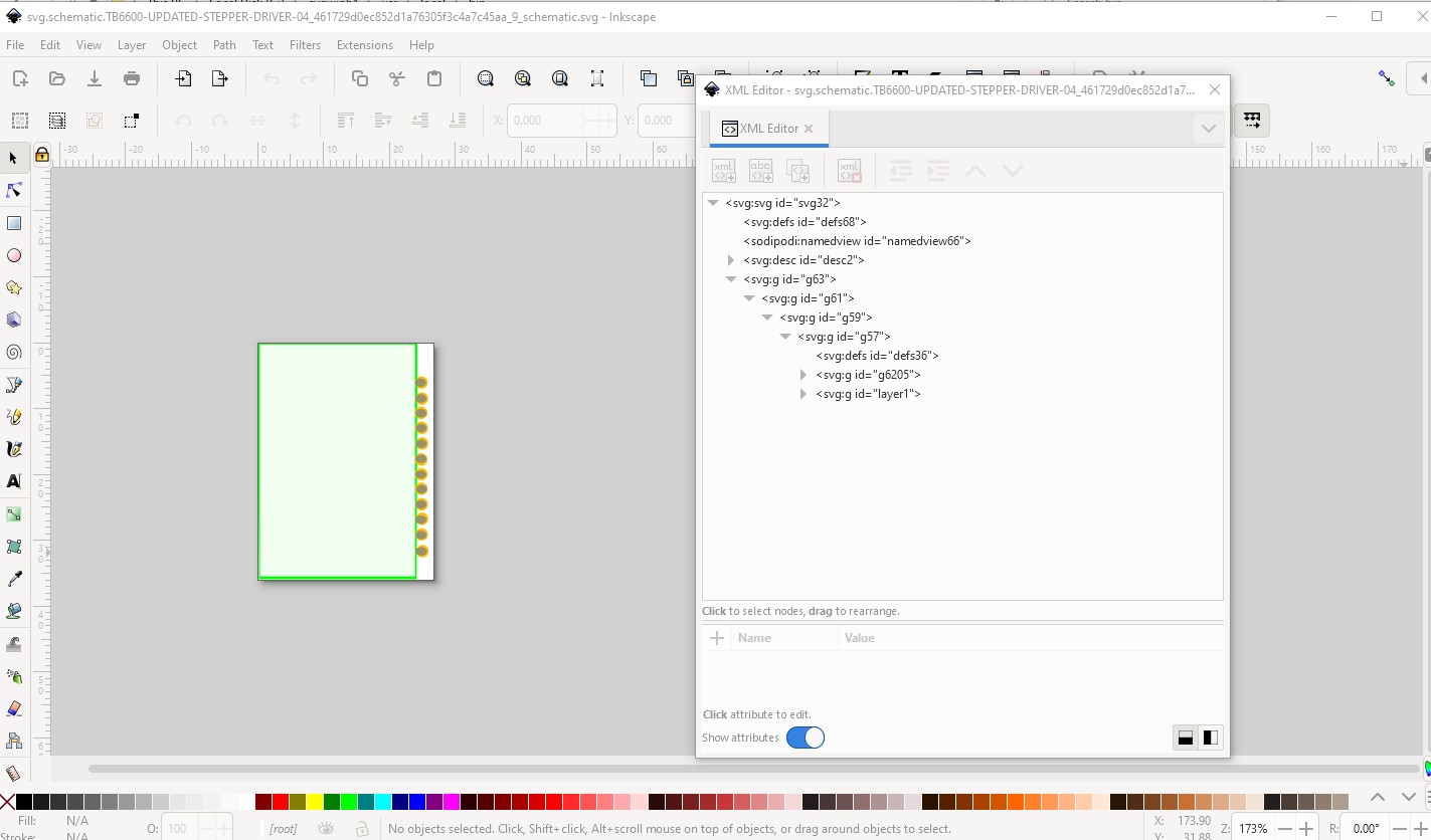
While this will work, it doesnā€™t match the standard Fritzing schematic so I choose to replace it with one generated by Randyā€™s Inkscape extension like this. First I selected the starting group and deleted it to leave a blank svg.

then started the extension and set the parameters

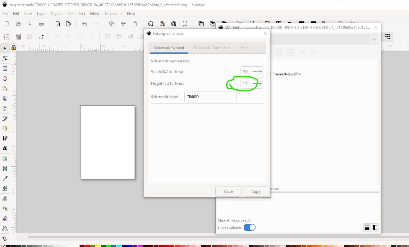
set the name in the label box set 0.6in as the width (turned out too small!) and 1.4in (12 connectors plus 1 space between them) for the height.

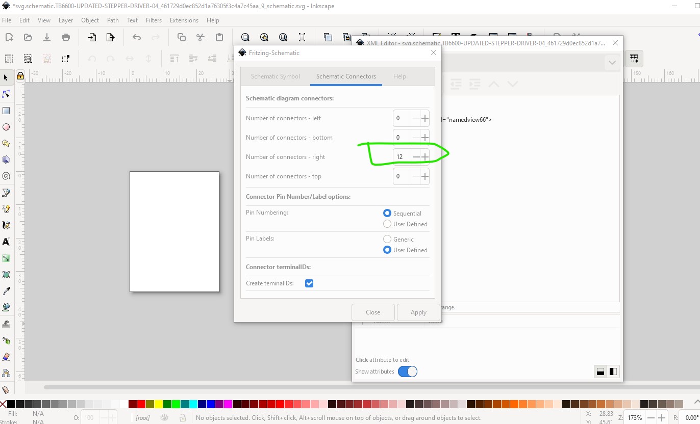
then set 12 connectors on the right (0 everywhere else) and hit apply

now enter the names of the pins, pin 1 is the bottom of the pins in breadboard here

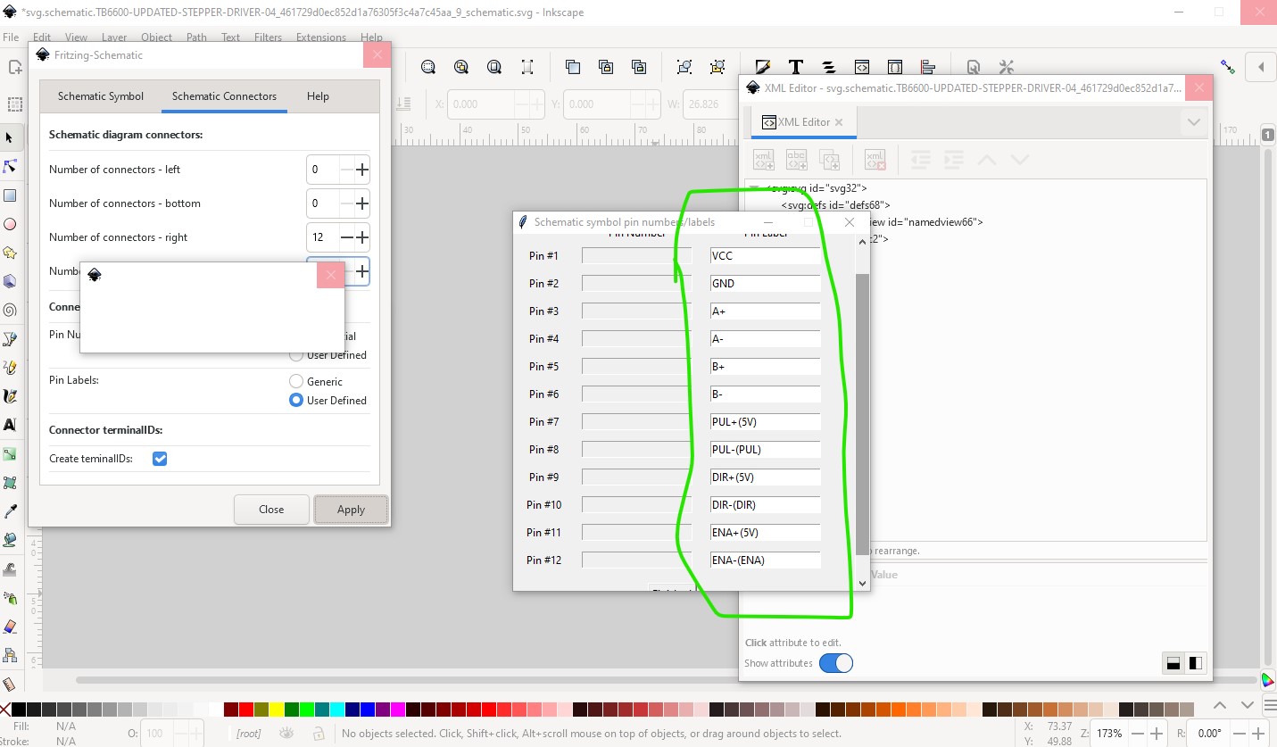
then click finished and it creates the svg

note it is to narrow so ungroup it to make changes

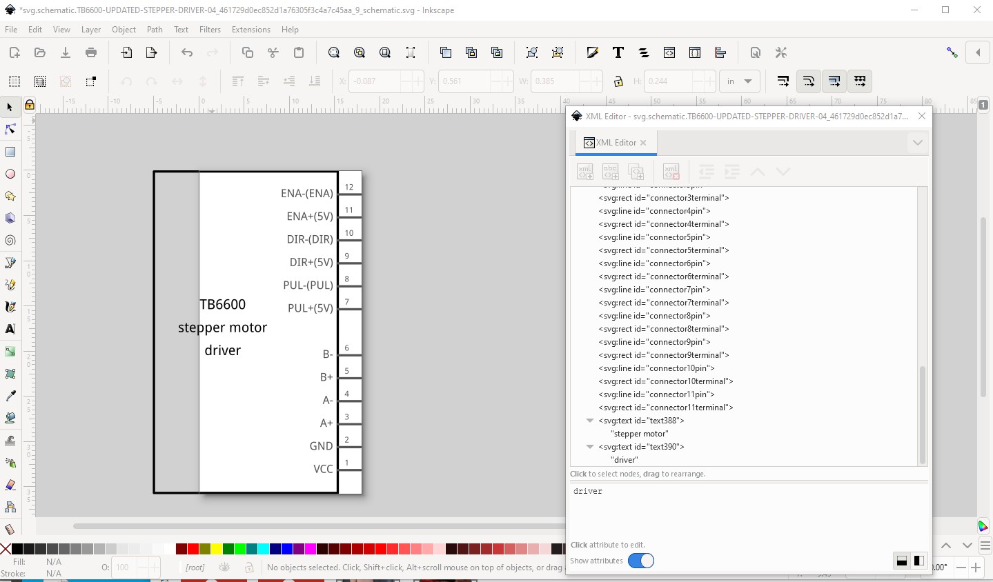
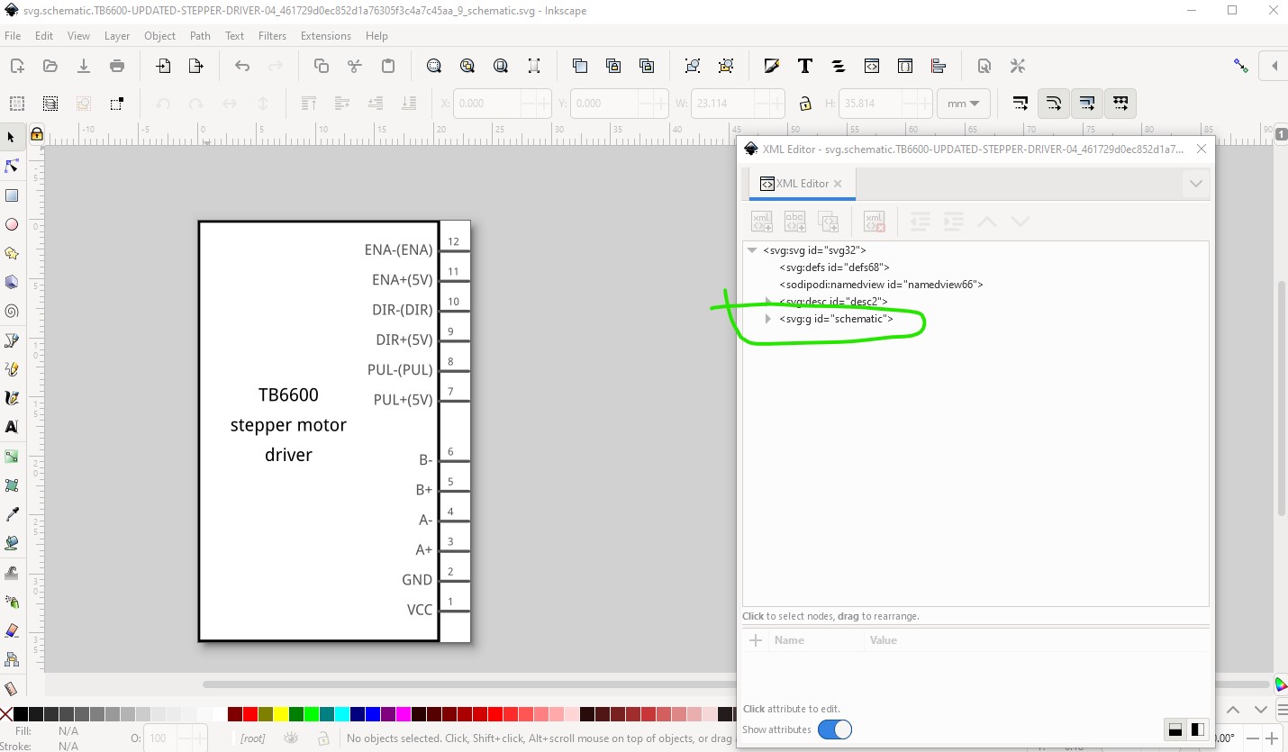
then move the bottom 6 connectors down 0.1in (to leave a space between the 2 pairs of 6 connectors) and increase the width to 0.8in and add some text. Now Edit->select all Edit->resize page to selection then Object-> group and set the layerId back to schematic and schematic is finished.

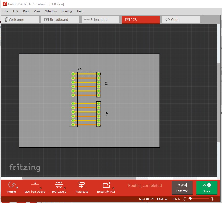
save it as plain svg and move on to pcb. There are two choices with pcb, we could suppress it entirely as they are all screw terminals (which donā€™t easily connect to the pcb.) Instead because the user may want to put an arduino on the pcb and interface it to the motor driver I chose to make pcb be header connectors that can then connect to the motor driver like this

that finishes off the svg files. Now on to the fzp file. There I chose to modify the file names to something more reasonable (and in the process changed the moduleId so this new part will load beside your original for comparison) I needed to change the connectors to start at connector0 and have labels that reflected the new pin positions. I added a url field to one source of the motor driver so people know where they can buy one. Finally I ran the resulting part through FritzingCheckPart.py to make sure it was correct (and to fix a variety of things that Inkscape does that Fritzing objects to!) which results in this new part

TB6600 NEMA-17-23 STEPPER MOTOR DRIVER-improved.fzpz (57.4 KB)

which looks like this in Fritzing

Peter

I will go through all that in depth tonight. ( A LOT to grasp ) Since I am not making a PCB with the
Arduino or Driver on the PCB, mine worked quite well in Schematic. It appears you completed my endeavor.
Thanks a heap.
I found that the 7805 Voltage Regulator in CORE Parts has a pin reversal between the Breadboard view and the schematic view. 7805 Pin Order should be (+in) (Gnd) (+Reg out) , left to right. ( the LEFT two pins ) disagree between views.
That error caused my Diode to short out in the schematic by connecting (Gnd) directly to (+in)
when the schematic auto-routed.
Thatā€™s why you commented about the diode earlier. I repaired the one I have, you need to note
that CORE needs that updateā€¦it is a very used part as an on-board regulator World Wide.
Thanks again for your assistance.
Bill

Iā€™m not sure this is a bug (it is certainly odd, but not necessarily a bug!) This is a Sparkfun part with an odd package type (to-220-alt) which may (or may not!) have this pin out. The standard 7805 part is in the correct order. As is this Sparkfun part

but this Sparkfun part (the one you used) is wrong at least in the pin order in the description (there may or may not be a variant of the 7805 with this pin order though)

Iā€™ll have a poke at it and see what I can find out and perhaps report it as a bug. A google search for ā€œ7805 ground in out pin orderā€ doesnā€™t turn up any chip with that pin order so Iā€™m inclined to think this is a bug.

Peter

I think you are right, regardless if you open up that part, the pins are misidentified between
Breadboard and schematic, I only noticed when you said I had a short.
I started using 7805 chips in 1978 I believe, and all that I have used have the pin order I listed. I was a ā€œControls Engineerā€ back then and designed in relay logic and early TTL logic to fabricate
some of the earliest PLCs. (50 years ago)
I started designing logic circuits in 1970, and adapted to CMOS (4xxx series), and even used
CPLDs from ATMEL with their logic design programs.
BTW I downloaded Fritzing several years ago in itā€™s infancy, It has come a LONG WAY since then,
a good bit friendlier, but I have a hard time following the SVG edits in Inkscape, Iā€™ve made SVG
with LightBurn (for my laser engravers mostly) since they came on the market. Much easier
and friendlier, and they have a tracing program that is simple for SVG. (but costly-30 days free)
thanks again, itā€™s normally tough to get help with programs,
Bill

Winder-Retrofit-WithTB6600-NEMA17-23STEPPER-MOTOR-DRIVER.fzz (107.6 KB)
I dropped the part you corrected in the Winder file, and Fritzing transferred perfectly.
( the 7805 I corrected is in here too) The Auto-route appeared to still work too, but I have not
cleaned it up or re-organized it yet.
Do you by chance have an external routine for converting the PC Board drill file to GCODE ?
I may just write one if not. I have MULTIPLE CNCs, 3D printers, and Laser engraver/cutters.
( mostly Home Built, some 25 years old )
I still get the error i had loading, so I still have to go through the earlier proceedure you
outlined for me.
Bill

No. but if you search the forum for cnc there are a variety of past posts I believe some with a reference to a gcode generator. When I route schematic on your .fzz file I see a number of problems.

One of the optocouplers looks to be missing a connection as the collector has no connection. The 5V from the arduino doesnā€™t seem to go anywhere as the switch is NO and there appears to be a short from NC to common which will cause the switch to not open. The two I/O pins connected together (circled in orange) arenā€™t necessarily a problem (as long as at least one is an input) but there doesnā€™t seem to be any reason for it and thus it may be an error. This is why I like to route schematic because it will turn up errors in breadboard that are not at all obvious. Here is a copy of your sketch with schematic routed

Winder-Retrofit-WithTB6600-NEMA17-23STEPPER-MOTOR-DRIVER-schematic-routed.fzz (120.2 KB)

Your sketch loads without issues for me, so if you are seeing complaints there must be still something wrong on your setup I expect. I would be tempted to export all the files in your mine parts bin as fzpz files (a good idea for backup anyway!) and then clear user files and reload them one by one and see which one (if any) complains. The reason I say if any is that clearing the user files may clear out something that was left over and is causing your problem. Iā€™ve seen cases where a file hasnā€™t been deleted for some reason and later causes trouble as Fritzing trys to load the same part again.

Peter

I saw a couple of the problems also as I checked the schematic. Corrected I believe. I found I did
not need the Regulated 5vdc, so removed it. I had a problem with the fuse on that circuit anyway,
It would not connect to the output side. ( bendable legs) I then added a fuse back in the 5vdc circuit from Arduino as a safety. Only the opto isolators use 5vdc, most of the operations are to
common ground, so the complete circuit has changed. That said, it also seems to load with no
issues. I finally removed the parts causing loading error. Itā€™s not ready to upload for your opinion
yet. It still has a lot of rearrangement and prototyping on an actual breadboard for verification.
The REAL breadboard is running perfectly right beside this computer, I am attempting to get the
Fritzing part to look like IT. There is a LATCHING operation to let Arduino know the desired
rotation direction for full travel until the supervised limit switch end of travel (reverse) is reached,
and the PULSE train follows the path of direction to actually operate the Stepper Driver in the
proper direction. The Enable is toggled to allow ā€œNo HOLDINGā€ so the motor can be effortlessly
moved for corrections by the operator. This also keeps the stepper from overheating.
ā€œStepper Holdā€ is not mechanically necessary or desired. This non-requirement stemmed from
the original actual operating circuit using an L298 that had no provision for relaxing the stepper
motor causing MASSIVE overheating when the machine ran slow. It was handled in programming.
This circuit keeps the motor much cooler with a LOT of reduced code, since the TB6600
addresses the issue far easier. Only a Tiny tweak in the programming code will allow me to use
THIS circuit on my SURFACE GRINDER that is currently Electra-Mechanically controlled. (relays)
Steppers HATE relays even WITH back EMF protection. I mainly want to use Fritzing
as a PC board lay out aid using my laser engravers to expose film. I have used negatives and
positives for many years, fabrication layout MANUALLY. Fritzing outputs are easily modified
to run in LightBurn I discovered by using their TRACING function. ( I have no GERBER )
Wish me luck
Bill

As long as you check schematic for errors, you should be fine. As noted it catches errors that are very hard to see in breadboard.

Peter

YES it DID ! I did a quickie with an isolated PNP NPN and it caught a wiring error to correct earlier.
Fritzing is starting to work well ā€¦ just need to verify PARTY DESIGNs !!
thanks a lot for your help. YOUR routing looked really good.
Bill

I just opened issue #367 on github for the two 7805 part with the wrong pinout (it appears they used the 7905 pinout rather than the 7805) and will submit a pull request to obsolete and fix the two parts.

Peter

Boy I really know how to find faulty parts. I found the Diode I used has directional problems as
marked and AutoTraces straight through ā€¦ it also wants to invert on autoTrace much like the
7805, so one window is flipped. The limit switches I tried to use failed much the sameā€¦ they simply
would not trace as configured. ( No matter , they are external functions and do not affect the
Printed circuit ) They as well need to be scrutinized in detail. So I picked 3 faulty parts from CORE;
what are the ODDS ?
I include the present level of the ā€œfzpzā€ file, An image of PC Bd screen, and an output screen
from LightBurn as the laser will print on Positive acting media for assembly. The circuit has changed considerably, added 2 opto isolators making a total of 4, giving me total isolation
from the real World. In this version I reversed the diode in Fritzing ( not in real World) to
keep it from messing up my schematicand circuit board tracing. I substituted the
LEDs with ā€œPADā€ like I used for interface to the real World ( forget what their ā€œtypeā€ is ) and most
problems disappeared. I left the Auto-Trace to the Arduino to assist me in naming the associated pads. I used the schematic you created for the TB6600 on the PC board for ā€œparallel wiringā€ of the real unitā€¦just ā€œWire to Wireā€ (except for 4 motor wires, with drill holes removed). . . the jumpers for it are already on the printed circuit board so a flat cable will hook it up without any detailed wiring directly on it.
There are several ways I can convert the output to laser, even direct image import. I include a copy of that as well. Check the DIODE, LED, Limit Switches, and 7805 since they ALL need updating.
Bill


Winder-Retrofit-Isolation-WithTB6600-NEMA17-23STEPPER-MOTOR-DRIVER.fzz (148.0 KB)

I donā€™t think it is necessarily the parts that are wrong. In breadboard LED2 is shorted (by a rats nest line) which indicates a bad connection in another view. Here the anode of the LED connects to pin 2 of the optocoupler but a rats nest line shows a short (from a incorrect connection in another view.)

capture

in schematic the anode of the LED is connected to the resistor rather than pin 2 of the IC thus creating the short.

When I delete both wires on the LED the correct rats nest lines appear from breadboard (and the LED needs to be flipped 180 degrees to connect correctly.)

dragging a wire from the cathode of the LED to pin 5 of the optocoupler will cause the short we saw. The correct thing to do is to do the wiring in breadboard then click in the rats nest lines in schematic and route the resulting wire correctly (as it will make the correct connection from the other view!) In pcb the LED is set to SMD and it appears that you used vias an pads to make a through hole part. A better bet is to change the LED to through hole in Inspector which will create the pads you want like this.

a better bet would be this

change the package in Inspector (lower right window) to THT like this

then route the traces directly. If you click on the package line in Inspector it will give you a list of the packages available. This one is for a 3MM through hole LED. Then back to schematic where the unrouted nets message indicates another problem.

The rats nest line shows a short across the switch. This is because of an incorrect connection in breadboard reflecting in to schematic.

This wire is incorrect, when I delete it the correct connection shows up as a rats nest line

although there is still an error somewhere as routing hasnā€™t completed.

moving the diode up one position causes routing to be complete except for pcb which still has unrouted rats nest lines.

Peter

Hopefully I am not so confused with all your help. I have another version that was designed for
my Knife Steel surface grinder. ( I am a Blade Smith so have to flatten forged steel ) This one
utilizes a similar circuit and program but has more toots and whistles. It has similar limit switching, and has a separate step controller for the Large stepper that it has to interface with.
[ direction of desired travel ] That will be optically isolated, not shown in MY circuit.
I changed out the Limit Switches due to failure to route, used Reeds instead, worked perfectly.
This circuit also has 2 OVER RIDE push button switches for one axis for set-up or correction.
The Arduino Uno Part has a similar problem as the actual unit. I have a programmed call for
A5 to light a diode (started out in program as something else that physically failed) and the schematic did it faithfully, however the PC board layout had other results. The last pin on the
Arduino is marked SCL, and pin A5 is marked as A5. Since itā€™s an obvious discrepancy, I would
like you to check the Arduino Fritzing Part. All other pins routed correctly. I used only parts that gave me no problems and /or replaced the ones that did, so routing went relatively smoothly,
and repairs were minimal. [ the ANALOG pins in this unit were re-defined as DIGITAL I/O ]
The board Traces were manually routed for this go, and oversize ā€œPadsā€ ( you have another name for them) were inserted for Arduino and TB6600 inter-connections. The components
and remaining Rats Nest were maintained for checking purposes against my operational
bread board Model and wiring diagram beside me. I have 3 type Optical isolator circuits
for impending machine isolation of other functions that do very little in this Board configuration
but are necessary for my equipment interfacing. I will try to send the latest Proto-part
to at least show you the I/O difference.
I could not find reference to addition of "OFF BOARD Equipment hook-up so manually added
ā€œPadsā€ and traces to have a soldering point for those. As I have time, I hope to find hints in the
forum to assist me in future projects.
Bill
Surface-Grinder-Isolation-WithTB6600-MOTOR-DRIVER.fzz (187.2 KB)

I just ran AUTOROUTE on the manually drawn board I fabricated from the routing lines.
I only saw it pick up the 3 jumpers I had put in it earlier.
Bill

There isnā€™t anything wrong with the limit switch in your original circuit. It should route just as well as the reed switch. If you can upload a sketch that shows the incorrect routing of the limit switch Iā€™ll see where the problem lies (as it doesnā€™t seem to be the switch part!)

The Arduino part is working as designed. The SCL pin on the Arduino connects to A5 internally (you canā€™t use both pins at the same time because they are internally connected.) In this image I clicked on the SCL pin at the top of the Arduino, as you see that A5 pin on the bottom also lights up because the two pins are internally connected. Fritzing routing will go to the closest pin in the same net. So a connection to A5 that is nearer the SCL pin will route to the SCL pin. You can fix that if desired by manually routing the trace to the A5 pin, but the autorouted solution is likely shorter as Fritzing selects the shortest route.

There isnā€™t directly an off board connection option. The usual solution is to use a generic header of the correct size like this. Here I dragged a generic header in to pcb (along with an Arduino Uno) and set the number of pins to 6 in inspector.

then in breadboard I set the header in the path of the wire to the Arduino like this

note you need to drag a wire from the Arduino to the pin header and from the breadboard to the pin header in order to get them both to connect, and thus it may be better to put the header in the breadboard like this

as it is less prone to missing connections. On the original if you move one of the wires on the header it will likely disconnect the header which will disconnect the header in pcb if you donā€™t notice it. As you see from the yellow dots the ground is connected to both the header and the Arduino. In pcb the header appears as pads and will connect to ground because it is in the ground net

In pcb I would suggest routing all the connections to make sure they all go where you expect. However there is a problem with that (which I currently canā€™t figure out!) If I right click on the wire I should be able to move it to the top layer (necessary because the off board wires cross each other!) But for at least some of the wires I canā€™t

This wire for instance wonā€™t move to the top layer when it should. This wire however will move to the top layer (as the other one should) and I donā€™t know why there is a difference, as the board is two layer (even though all the traces are on the bottom layer!)

and the wire will correctly move to the top layer.

I canā€™t see (and donā€™t know of any setting that will do this) how some wires are only bottom layer. It makes me wonder if you have database corruption again (although this is a very odd form of it!)

Peter