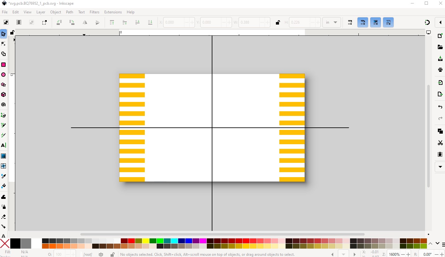
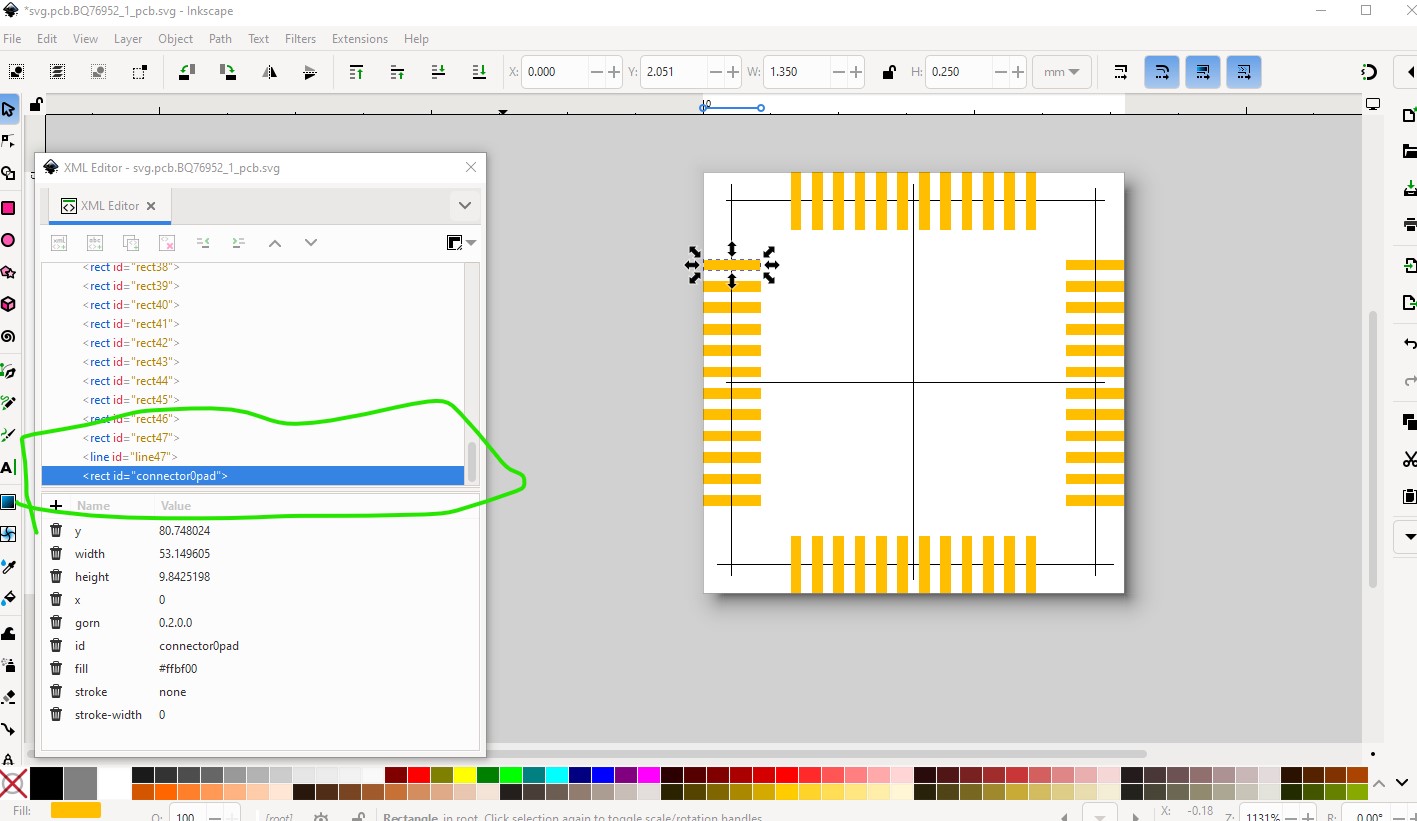
Seems odd, I have never had a problem with Inkscape that way. Of course I’m on Windows10 not Linux so X isn’t a factor. In any case construction lines are your friend. Here is the start of your footprint and how I did it. I started with a single pad 1.350mm wide and 0.250mm high then set that at 0 0. Then added 0.5 mm using the tool bar to create 12 pads, then duplicated that and moved it 8.5mm in x to get this
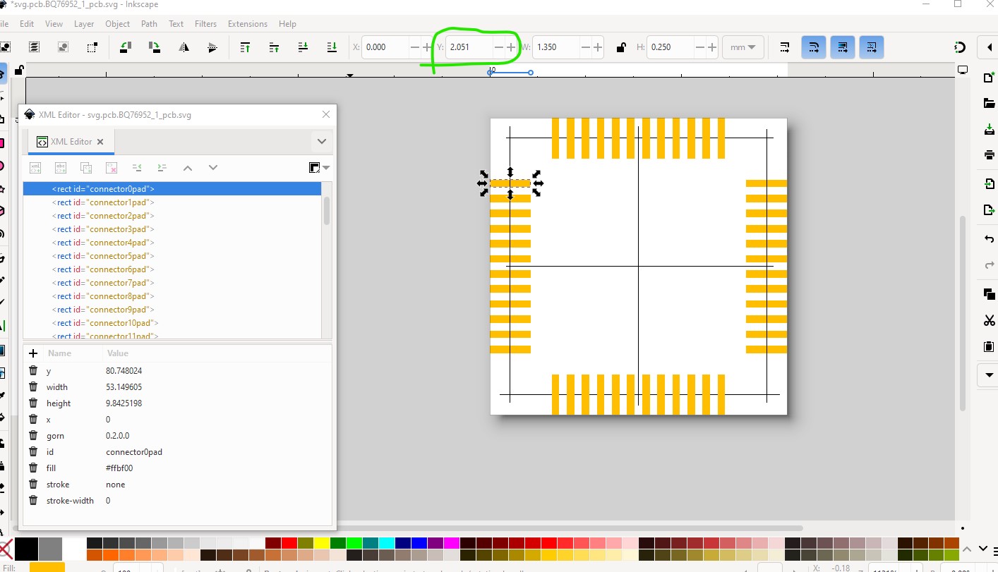
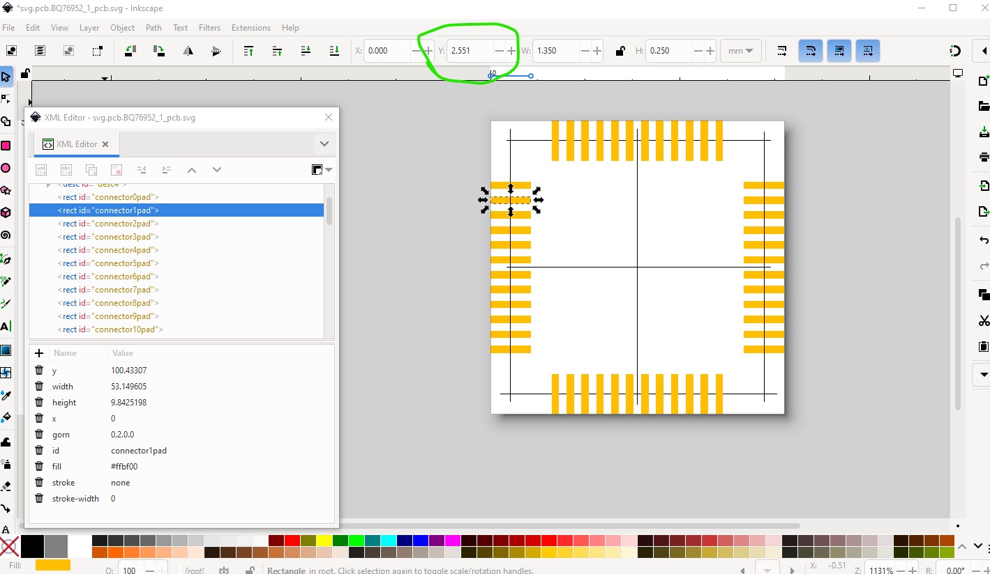
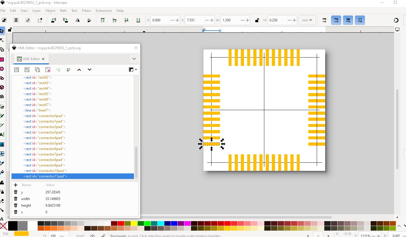
then created and centered the construction lines (1 thou in wide) on both axis. From the center lines add the pad center lines at+/-4.25mm (- 1/2 line width!) then center the middle 2 bottom pads and dup and move the pads (0.5mm at a time) til you have all 12 on the bottom. Dup them all and move them up to the top. Starting from connector0pad in this image, dup it and add 0.5mm to its y coord like this 2.051 in y becomes 2.551 to move it up 0.5mm as is required.
the only pin the needs a label is connector0pin. I have a python script that will renumber the following pins in order no matter what they are labelled. A part should be up in a bit.
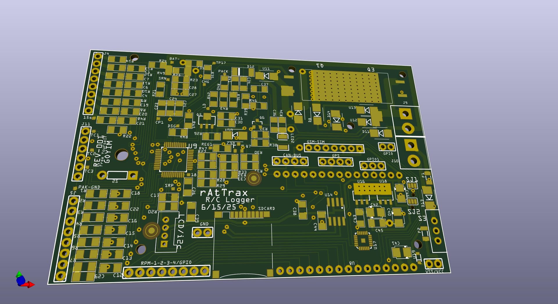
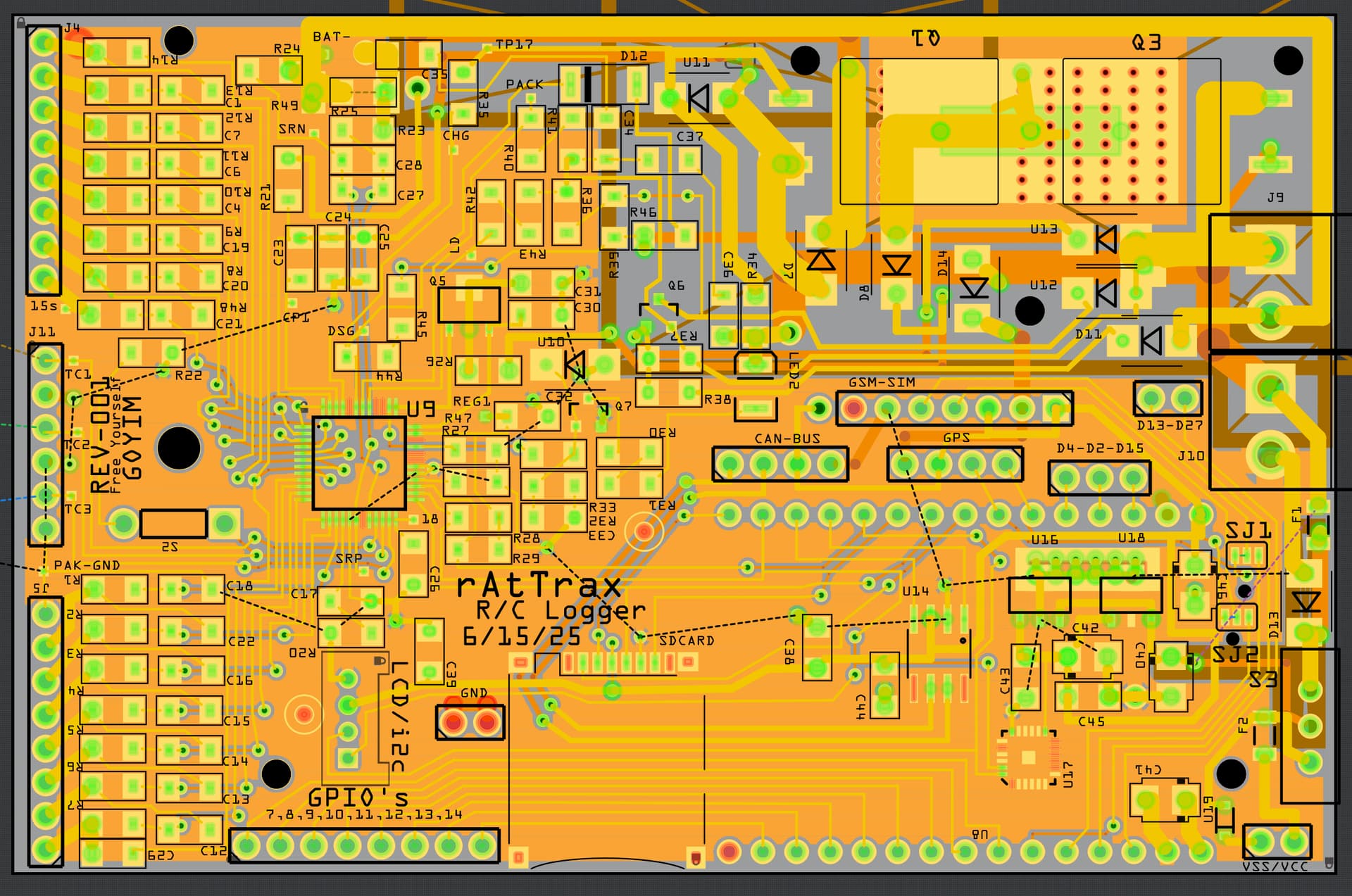
This part should do what you want. To route the traces you need to set the grid size down to 0.5mm (the pitch of the IC.) Again you need to set DRC down to 0.07in of clearance to get DRC to pass.
Made some awesome progress with this footprint, PCB designed and produced. BIG shout-out for the help! Much appreciated, and I’m sure my project will as well! Ha, super awesome!!