Hi guys,
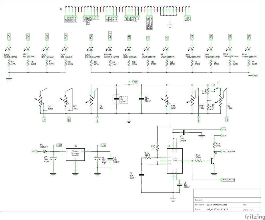
It’s my very first time that i use fritzing, so expect some beginner mistakes :). I’ve just made my first scheme:
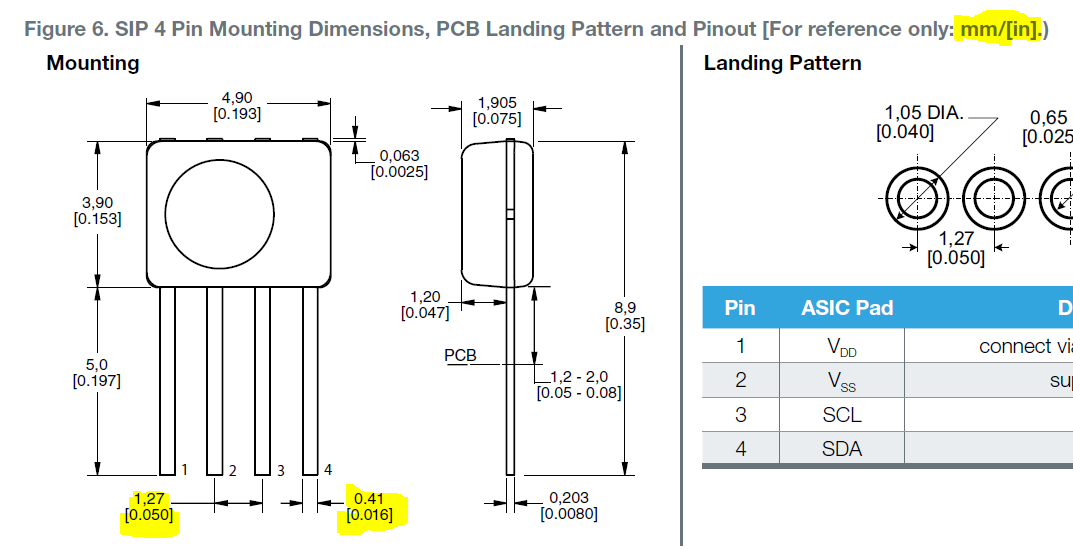
The 4 pins circled in red is actually a honeywell humidity sensor. (HIH8000 series, sip 4 mounting) I couldn’t find this part in the parts library, neither on the internet so i just ‘simulated’ it by placing headers. What i was wondering is, are the headers that i’m using right now the same ones as the standard ones that you can break of? I would post a picture but fritzing doesn’t allow me to post more than one picture because i’m a beginner -.-
If you see any other rooky mistakes in the scheme please tell, because i’m planning to print this one 
Thanks!
If it’s 4 pins at 0.100" just use a 4 pin header from CORE bin, as it will better in PCB view.
EDIT
Make sure there is a big black dot on junctions or it might not actually be connected, and always make sure you see a black line between components. That 24LC256 looks a bit weird connection wise.
1 Like
Thanks for the quick reply!
I know th 24LC256 looks strange at the output connection. It’s very frustrating but i can’t get the connection dot to appear on the grid point. It always keeps jumping between two grid points. I’ve no idea why, but connection-wise it’s okay if i hover over it with my mouse then everything turns yellow.
Do you mean this header: 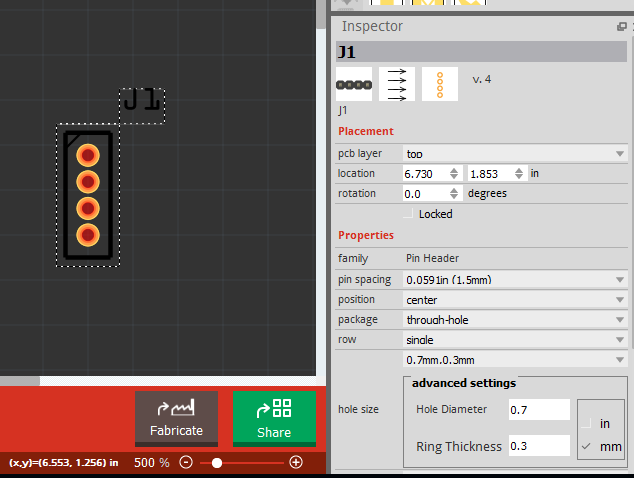
I adapted it for the pin spacing of the sensor, do you think that it’s a problem that the ring thickness is only 0.3mm?
Maybe this makes it a bit clearer, this is my sensor:
EDIT: i now see that next to it there’s a pin landing drawing  , gotta love this data sheet, they even use a ring thickness of 0.2 so i guess it’s no problem.
Yeah, you just select pin pitch and ring sizes in the Inspector for the header.
0.3mm I don’t know, but there isn’t much holding it down. Maybe a smaller hole as the pin is 0.4mm.
I like to see a black line between 5V/GND and the IC, it makes me feel better.
Even the other side of the chip I would come out 1 grid so I can see the connections better.
Be careful when you join to a junction. I usually grab the junction and move it around to make sure everything is connected - you have to do it anyway because it looses the snap -.
You can set grid spacing and turn grid on and off in the top menu under View.
Hi guys,
I tried to make the schematic better, but i don’t understand the black dot system. As you can see here when i highlight it everything is connected: 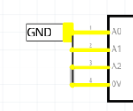
However if I don’t highlight it then i have three different kind of dot’s. You have the big black one (which i trust the most), than the small black one and even a small green one. What is the significance of all of them?
Sorry image had to come in the second post because i’m new -.- (what an annoying rule)
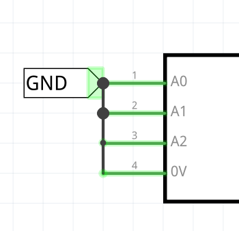
The small dot on 3 pin is telling me it’s not a 3 wire junction, and it’s connected because you have 2 wires directly on top of each other. Big dot is 3 or more connections.
Move GND label 2 grids left.
Then move the vertical connection line 1 grid left so that every line travels 1 grid left and then up.
On mine I never have a green to green connection but make sure I see a black line between both. It’s not essential, but it is good practice because it has caught me out before.
1 Like
Hey Old Grey, sorry for the delay (i had and have exams )
What do you mean with a green to green connection, is that two green pins immediatly connected?I now remodeled the schematic, this is how it looks like right now what do you think? If my definition of green to green is correct, then this one should be okay.