Nice job on breadboard view! A couple of minor issues, on this one you haven’t bussed the 3 ground wires as you have in the 3.0 version. Schematic has pins not aligned on .1 centers which makes it messy to connect to other parts. Personally I like to set inputs on the left and outputs on the right and align schematic so that a row of header connectors in breadboard match the same pins in schematic (which you have mostly done except for a few cases as shown in the sketch below).
If you click on one of the grounds in the 3.0 part it (and all the other grounds) will turn yellow (on the 2.0 part they don’t because they aren’t bussed). That is because they are set to be bussed (connected) together internally in Fritzing (as they are in real life). If you are editing the underlying files (as I usually do) you need to add a bus section to the fzp file. If you are using the parts editor then this recent post in another thread (currently the last post) tells you how to do it in parts editor:
Yes, typically schematic parts are on a multiple of .1 inch centers so that schematic looks neat and all the parts match up.
Unfortunatly no, that one is a Fritzing quirk / bug. It sometimes gets the orientation wrong (and sometimes doesn’t align parts to the grid until you move them) and you just have to manually rotate it to get it the right way.
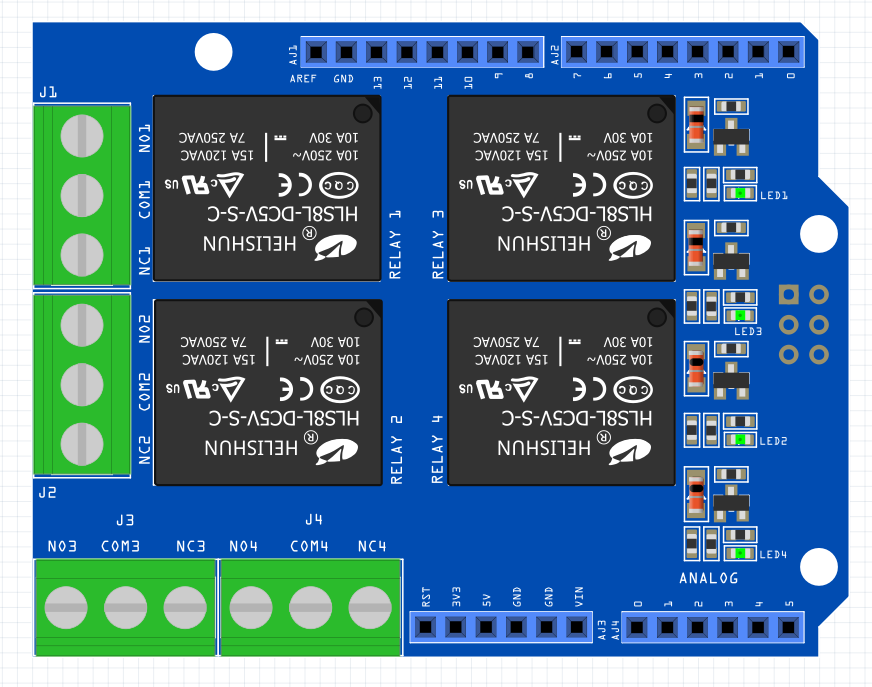
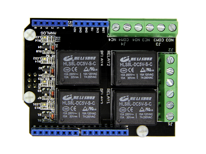
Hi, finally got it done. The schematic svg was messed up big time. Not sure what happened but I think it’s good now. Take a look and let me know if there are any more problems.
Still some problems. Schematic is I think at 90dpi (because fritzing aligns it to the grid correctly) but it loads in Inkscape .9.2.1 as too small (because it thinks px scale is 96dpi I expect). This is happening because the view box height / width are in px. The solution is to (assuming it loads in your editor at the proper scale) change the view box height and width parameters to in or mm. To do that edit->select all then change the tool bar to in or mm and copy the height and width parameters (in in or mm) from the tool bar in to the height and width parameters adding a trailing in or mm to the value in the first element of the drawing using xml editor. When you press set it will rescale the drawing to the real world coords which avoids the px confusion. For reasons I don’t understand your terminalId definitions are being ignored (that is why the schematic lines in the sketch below terminate in the middle of the pin). That said the correct terminalId values appear in both the fzp file and the schematic svg. Ah! just saw it, your terminal ids are mostly paths (which don’t work as terminalIds. The couple that work are polygons which do work although I prefer a rectangle with height and width at .01 in. I don’t think fritzing can calculate the center point of a path to know where the center should be so it defaults to the center of the pin (which isn’t what you want).
PCB has a couple of problems: the holes for the pads are .035 (IC size) they should probably be .038 (.1 in header post size). The board outline (which I think is one of the polygons) has a fill value set. It probably wants fill:none and a stroke width (although I don’t know how to do that on a polygon) to draw an outline around the board. As it stands the entire silkscreen layer is one color (the fill from the polygon) and the lettering is wiped out. Isn’t parts creation fun Below is a test sketch that shows the pin alignment problems in schematic (and an easy way to test that the pins all have correct terminalId defiintions.)
Wow, I use Illustrator, I tried Inkscape and It seemed less intuitive than Illustrator. I couldn’t even get any layers to show up when I opened the SVG file. I may try it again.
Do you think inkscape is better than illustrator for these SVG files?
Seems they both have problems from what I’ve read though not sure how to change the view port in Illustrator unless Illustrator calls it art board then it is already in mm so I’m at a loss on that one.
I’ll read over your comments carefully and see what I can do to fix the issues. I did use the eagle2fritzing program and did very little to change the PCB layout as I don’t use it but I’ll see what I can do.
Inkscape’s main feature is that it is open source and thus free , I use it for that reason and because a lot of our folks use it but which ever one you are comfortable with should be fine though. I don’t know how to set the parameters in Illustrator, maybe someone else will though. Here is the xml that you want to change (from editing your schematic xml file) in case that tells you what to change:
<?xml version="1.0" encoding="utf-8"?>
what you want to do is replace the width=“108px” and height=“165.6px” with the equivelent in in or mm. Then the scale is set without fritzing needing to guess at how many px per inch is being used. It isn’t vital because Fritzing appears to be guessing correctly as the part is properly scaled, only Inkscape is having problems. It looks like you have an older illustrator that is using 72dpi as px as changing the height / width in Inkscape to height 2.3in width 1.5in (calculated by dividing the px values by 72) looks to fix up the scaling in Inkscape. The main issue is that terminals defined as a path don’t seem to work, so replacing them with either a polygon (such as connector12terminal) or a rectangle will fix that. Setting fill to none with a stroke width set to make an outline around which ever polygon is making the board shape should fix the silkscreen problem (not that I know how to do that in Inkscape let alone Illustrator though ) one of our more experienced board makers may know how to do that though. In Inkscape the hole size is set by stroke width and hole diameter. The current values (in Inkscape) are diameter .065in increasing that to .068 will make the hole .038, but it (at least in Inkscape) will also move the x y coords a bit and misalign the board. I usually use the xml editor to figure out what the new radius should be and manually change that (which keeps the x/y coords constant in Inkscape).
edit: A bit of experimenting in the pcb svg indicates that setting fill=none in the polygons and path in group silkscreen XMLID_1_ g6 and g10 and path13 fixes up the silkscreen problem.
 Below is a test sketch that shows the pin alignment problems in schematic (and an easy way to test that the pins all have correct terminalId defiintions.)
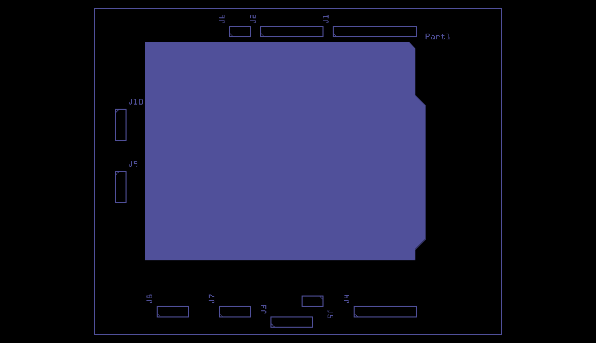
 , I use it for that reason and because a lot of our folks use it but which ever one you are comfortable with should be fine though. I don’t know how to set the parameters in Illustrator, maybe someone else will though. Here is the xml that you want to change (from editing your schematic xml file) in case that tells you what to change: