Thank you for fixing so many things on the sketch. I won’t be able to test this connection physically because I don’t have them parts because I am using the 6n138 optocoupler with the 1n914 diode. The only thing that has caught my attention is the midi out going through the optocoupler. I don’t need it to, I only needed the midi in to go through the midi in.
Anyway I have had a go at the schematic view and have everything routed but I’m not sure if it’s correct. But since doing the schematic view the breadboard view isn’t fully routed. One of the capacitors has a rats nest on it. I only need the capacitors for the led ring and strip. I have one going across the power rails of them. Do I need both of them? Chewie 2_fixed_2.fzz (120.7 KB)
The 1n914 is the same as the 1n4148 so no problem there, you only need to get a 6n137 to change to that if you choose. The posts I saw on the 6n138 say that the slow rise time because of the open collector output some times cause serial errors on the mega UART which manifests as either no midi output or the wrong command because of an error in the serial data coming in. If you don’t see this problem the 6n138 should work fine (unfortunatly it may work fine most of the time but fail sometimes which is why I would use the 6n137 solution.) The resistor connected to pin7 on the 6n138 is intended to speed up the rise time of the output, but getting a proper value may need you to have an oscilloscope to look at the wave form (which you probably don’t have). A way to test this if you can arrange it is to have the midi device that connects to din2 to send the same midi message over and over to the mega. On the mega you would need to write code that receives and checks the value of the midi message. If the message is the same every time and none of the messages are missing (based on time or a count of how many messages the midi device sent) then you don’t have a problem. If messages are missing then the 6n137 (which can be tested the same way) is probably a better bet. As I said I’d use the 6n137 because it is likely to be more reliable and simpler (doesn’t need the tuning resistor) but either will probably work.
Then you can delete din1 and its associated resistors completely as its only purpose is to pass the received data on to the next midi device. That simplifies your board by a bit.
That is because there is an error in schematic. If in schematic view you click on any +5V or ground connection you will see that both +5V and ground connections highlight yellow indicating there is a short between 5V and ground which is causing the routing problem in breadboard. It looks like you moved the top neo pixel part at some point and that moved the wire from +5V that should go to the neo pixel part to ground causing the short and the routing problem. As well a number of other parts were moved creating non straight lines. To avoid this problem you may want to lock the all the parts by clicking on them one at a time and clicking “lock part” with that set you can’t move the part by accident (and need to unclick it if you want to move the part).
If both neo pixels connect at the same place you can probably only use a single capacitor at that point. The reason for the large capacitor on the neo pixel is that they draw a lot of current, and the current draw varies with time (as the individual clocks in the neo pixels drift in time). I would use separate wires from the power supply (which needs to be able to source the entire current drawn by all neo pixels being on at the same time because that will sometimes happen!). I would be tempted to put a 1 amp or higher schottky diode (for low diode drop) followed by a 100uf capacitor between the power supply and the circuitry other than the neo pixels. What can happen when the neo pixels all come on at once is that the 5V line will momentarily drop below 5v (the 1000uf capacitor is supposed to stop that but it may not be able to do so) and that can cause the mega to reset or otherwise malfunction sometimes which can be very frustrating to find. The shottky diode blocks the drop from the neopixel getting to the mega and the 100uf cap supplies power to the mega with a steady 5V until the power supply catches up again. Another alternative is two power supplies, one that supplies the mega and one that supplies the neopixels, but the first solution is cheaper and easier. Below is your sketch with the various lines straightened and the short removed and rewired to the neopixel correctly.
I have ordered some 6n137 optocouplers, so they will take a few days to arrive and I will then test the circuit for the midi in and out you drew. I don’t have a oscilloscope so I can’t test the wave form. But I’m sure it will work, I will test the 6n137 optocoupler anyway. As long as the messages are sent it’s all good. Because the leds are controlled by midi using scripts in a program. The neo pixel and the led strip are over to the left hand side of my project so they will most likely be together. So I could probably use just a single capacitor, I will have to have a look at maybe using a schottky diode. Thank you for updating the sketch, how can I move on now to a pcb. I really want to progress to pcb, I’ve never made one before so it’s all new to me.
I expect the messages will be sent correctly, the problem is that they may not be received at the mega correctly. The errors that were reported with the 6n138 are that the rising edge is too slow (because it is being pulled up rather than driven up). That means that while the midi device probably sent the message correctly, the mega doesn’t always receive it correctly. Since the source of the midi messages is a script it should be fairly easy to test this. Modify the source script to send the same midi message something like 1000 (or even 10,000) times. On the mega create a program that reads incoming midi messages, compares the message to what should be sent (and counts an error if the message received doesn’t match what was sent, easy to do when always sending the same message, if it doesn’t match at the mega, then an error occurred in transmission) and counts correct messages. When the source has sent its 1000 (or 10,000) messages check the count on the mega and see if the good message count plus the error count match the number the script sent. It they don’t match then some messages were lost completely.This may take a long time, but you can run it overnight (or for a few days if needed) to see what the error rate looks like. This would also be a good tool to keep around, in case you run in to a situation where messages look to be being lost. If you run this program on the link where messages are being lost it should tell you if the errors are occurring on the serial link (as opposed to somewhere else in the system). If the mega doesn’t receive all the messages then you have the system error rate and you can decide if it is acceptable (a couple of losses in 1000 is perhaps acceptable, 500 losses in 1000, i.e a 50% error rate, probably is not). Doing the same test with the 6n137 installed is also worthwhile to see if it has a lower error rate.
Note Old_Grey’s comment on making changes when more than one view is routed. At worst you have the current version to fall back to if a change in pcb breaks the other views. I’d advise keeping a copy of working sketches as you proceed so you don’t lose a large amount of work to an error that corrupts the database. Start by positioning the parts in pcb view in such a way as to make routing easy. Unfortunatly it is trial and error (and autorouting works so poorly that it isn’t worth even trying for a board like this!). If you find that you can’t route some traces, see if moving one or more components around will make routing easier. It is hard and experience is the only way it gets any easier. You can also always post your current sketch and one of us can tell you how we would do what you want to do (as a first board that’s what I would do, one of us can probably make a suggestion that will save you a lot of trial and error). Once its done, before ordering boards post the final result here for some of us to check for you as it is easy to make mistakes that produce non working boards. Good luck!
I have made the original sketch which I sent you originally it is how I have my circuit currently set up. It is good to have because I know that everything is working with this circuit. I know you have helped me greatly, and suggested some changes that could be beneficial but I’m not sure with which circuit I am going with. If I’m honest I don’t want to be moving parts now when everything is working as it should be. It’s took me just over a year and a half to get this project somewhere close to the end. I just need to move onto the pcb now and then I can get everything cased. I have started to attempt the pcb view but it is a mess but everything is routed. Please would you check my drawing and the connections on it? I think the pixel strip isn’t correct in the schematic view. Thank you for your helpChewie original circuit.fzz (156.0 KB)
Yep, you look to have moved the neo pixel in schematic and that broke the +5V connection (the end of the wire going to the neo pixel doesn’t connect to anything. As well the 6n138 is incorrect wired in breadboard. The chip needs to be rotated 180 degrees (the current one is the correct direction for an IC which is wrong in this case). To fix that I deleted all wires connecting to the 6n137 in schematic and pcb then in breadboard clicked on the 6n137 and rotated it 180 degrees. That gets the pins in the correct place for your working circuit. As well the wire in breadboard on din pin 5 was in the incorrect place. It should go to pin 3 not pin 4 (which is nc). I also moved a couple of the wires in breadboard so there weren’t two connections on one pin (which won’t work on the real breadboard) but they are cosmetic. With those corrected you should now have a working copy of the original circuit as it is on the breadboard. here (I didn’t finish pcb however). PCB looks somewhat OK as far as routing goes, but a few suggestions:
Board houses charge by the square inch, so a bigger board is more expensive. In this case I’d probably mount the mega on its own (to save board space) and run jumpers or perhaps fit the circuitry in to a mega shield format and put your parts in the shield (to save the cost of the space for the mega on the board). As well you want to group the components as close together as possible (with still being able to route the traces) to minimize the cost of the board. Note if you are putting the board in an enclosure, you need to be mindful of the dimensions of the enclosure and add holes to the pcb to allow it to be screwed in to the enclosure.
currently the pot over lays the neopixel which you probably don’t want in practice. In fact probably the neo pixels want to go to header connectors because I would guess they will be somewhere remote from the board.
The usual advise for pcb routing is horizontal and vertical traces with no right angle corners (bends should be at 45 degrees). This mostly mattes in RF circuits and right angle connections would work fine here.
As noted the neo pixels take high current so their power leads should be separate from the power leads to the rest of the circuitry and be as wide as possible (to increase their current carrying capacity. I would actually not put the power wires on the board at all but run a large gauge wires from the power supply to the ground and +5V pins on the neo pixels. In all you look to be doing pretty good .
Thank you for taking time to look at my circuit and fixing it. I did indeed move the pixel strip in the schematic view. Because I noticed the pins were green but the ground wasn’t. So I moved it and the lines appeared but the ground pin still isn’t connected. Is that right? because I have the ground pin connected into ground on my breadboard. Thank you for the advice I will try and keep my traces horizontal and vertical with 45 degree angle connections. I have an idea the size of my enclosure will be, but not exact yet. I am going to try and make it as a shield for the mega. The reason why I have my pixel ring on top of my pot is because that is how the final design is going to be. the pot will go through the pixel ring. But I think I am going to connect them by using wires from the pcb.
I’m sorry I don’t fully understand what you mean with point 4.
As noted the neo pixels take high current so their power leads should be separate from the power leads to the rest of the circuitry and be as wide as possible (to increase their current carrying capacity. I would actually not put the power wires on the board at all but run a large gauge wires from the power supply to the ground and +5V pins on the neo pixels. In all you look to be doing pretty good .
Moving the part is one way to correct that problem, but you then need to check all the connections on the part to make sure they are all connected (in this case they weren’t which caused the problem). I expect the +5V connection to the neo pixel was not actually connected to the neo pixel in the original sketch. When you moved the neo pixel because +5V wasn’t connected that connection didn’t move with the neo pixel (because Fritzing didn’t know it should connect there) leaving the +5V connection unconnected with the wire hanging in space (and that in turn reflects in to breadboard and schematic view potentially causing problems there as well). Worse, if that dangling wire contacts a pin on the neo pixel (which it didn’t in this case) it will make a connection there where you don’t want one. If you put the cursor on the pin of a part (for example the +5V pin on the left of the top neo pixel) and left click the mouse button all connections will highlight in yellow. In the example the +5V wire on the neopixel, the T that denotes the +5V net and the +side of the capacitor all turn yellow indicating that these three points are connected together as they should be. After moving a part you should check all the pins to make sure that the connections all still go where they are supposed to. If you try the same thing on your Chewie original circuit.fzz you will see that the schematic looks (and is) incorrect, although it is not quite as incorrect as it first looks (likely a Fritzing bug here). If you left click on the ground pin the - terminal of the cap, the ground pin and the ground pin of the neopixel all light up yellow indicating a connection, even though on the screen the ground wire to the neopixel ends below the neopixel and does not appear to connect. Same with the di pin, while it appears on the screen to connect on or near neopixel ground, it really is on di. Selecting the neo pixel and moving it slightly causes the screen to update correctly showing the di and ground connections (with ugly wire layout) and the +5V neo pixel unconnected which is what pcb view is showing. I usually prefer to lock the parts in place and either move the wires til I get a correct connection or delete the wire and rerun it to get a connection. The click to highlight the connections to this net (which works in all views) is a very useful tool for insuring you have all the connections you expected to. It is how I find these errors when a sketch is doing something unexpected.
Ah! now it makes sense. Either method (mounted on the pcb or connected via wires to the pcb) should work as long as the pot selected will fit inside the neo pixel ring (I assume there is a hole in the center of the ring). Then which ever method is easier mechanically is what you should do. If the enclosure has a lid where your board and the mega under your board can connect with the neo pixels the jacks and the pot will all come out one plate that should work (although it depends on the position of the holes in the enclosure plate exactly matching position on the pcb which can be a pain to do, with wires to the board the enclosure holes are independent of the panel hole dimensions as wires will bend unlike neo pixels or jacks soldered to a pcb . I usually opt to use wires to make my life easier but either will work.
The issue with the power wiring to the neo pixels is voltage drop at high current. The neo pixels sometimes when many or all the leds are on and the clocks align (which will be only sometimes) draw a lot of current. That current in turn causes voltage drop in either the wires or the PCB traces (which are effectively wires on the board). A high current caused voltage drop in the ground wire can reduce the noise margin for a low level (which is only .7V) and cause intermittent (and thus very hard to find) problems in the logic circuits and the mega. One way to avoid that is to run the power and ground wires for the two neo pixels from the power supply directly to the neo pixes (and the 1000uf capacitor which wants to be as close to the neo pixels as possible. The power and ground for the logic then uses a different set of wires (or traces on the pcb) also connected to the power supply at only one place You do not want to have two paths to the same point in any circuit (although it is most important in the power traces) as this causes a ground loop if the current causes a different voltage drop on the two halfs of the path which it will if the resistance of the two paths is not identical. Its best to not have any loops in any trace.
The way I deal with this (when I remember too, too often I make one more change before doing a backup and end up losing work) is to keep copies of working sketches. A version control system such as git, while complex to learn makes this relatively easy. Alternately (and much easier if you remember to do it) is just save a copy of the sketch to a new file name (whose name will tell you what state the project was in when it was saved). To make changes copy that sketch in to a new .fzz file with a new name and make your changes. If you screw it up (which I do all to often)
you can go back to the saved file and try again. If you are successful with making some number of changes, again save that working sketch in a new file name (this is what I’m typically don’t do ) so you can go back to the saved copy when you screw up.
As well something I did but didn’t mention: in pcb view you should click on routing->Design Rules Check (DRC). This will check the clearances of all traces in the pcb (it finds a lot of problems in your current pcb!). For a board this simple the standard rules should do just fine, although the pot inside the neo pixel part will generate an error that can be ignored. It looks like some of your traces are too close to each other.
The pot does indeed fit inside the pixel ring because it has a hole in it. I have spent hours moving parts around on the pcb. At one point I had it right by going into Design Rules Check. I had no issues. Since I have moved the parts, I now get an error with the neo pixel strip. About the pixel strip should have both top and bottom copper layers. I can’t seem to get past this error.Chewie original circuit.fzz (124.1 KB)
This is fairly easy. You are using the original neo pixel part which is broken (among other things it doesn’t have copper1 or copper0 I don’t remember which). Looking at my corrected part I see there is a scaling issue in breadboard which I will correct and post a new part in a bit.
OK, starting from Chewie original circuit.fzz above do the following to correct the sketch:
In breadboard we see that the neo pixel 30m strip is connected wrong (the wires don’t match). As well this is the broken part pcb
doesn’t work and the labels are wrong. So I have created a new part that corrects the errors in the original (and the one that I
fixed earlier). Now you need to replace the current one (in all your sketches, not just this one!) with the new part. To do so:
Open the sketch Chewie original circuit.fzz in Fritzing
in breadboard view select the neo pixel part and right click it. Then click Delete Minus (not Delete but Delete Minus) this deletes the part but leaves the wires.
In the mine parts bin right click on the neo pixel part and click remove part. Answer yes to the do you really want to remove this part prompt.
Exit Fritzing and answer save to all the dialogs that come up (you want to save the removal of the broken part so it won’t be present anymore).
Restart Fritzing and reload the sketch. There should be no neo pixel in any of the views and no neo pixel in the mine parts bin if the above has completed correctly.
File-open and load Neopixel_Strip_White_30_m.fzpz which is the new part. The neo pixel part should appear in the mine parts bin.
Drag the new part in to breadboard view and move the wires til the connections are made. Check the connections are correct by moving the new part a couple of spaces to the right, if the 3 wires expand to folow the part the connections are correct and breadboard is done.
Change to schematic view.The new part is misaligned and has rats nest lines leading to it. Select the part and move it to the correct position then right click the part and click lock part to lock it.
Delete the 3 wires that should connect to the neo pixel to leave only the rats nest lines.
Click on each rat nest line and move the mouse a bit. This will cause the wire to be created to the connection point. Now click on the bend points on the wire and move them to the correct position.
Once all the wires are correctly placed left click on each of the 3 neo pixel connections and verify all the connections light up yellow.
12)Now switch to pcb view and move the neo pixel part (which will be off the board somewhere) to a clear area on the pcb and routing should then work and drc will pass.
At this point save the sketch as a working checkpoint file. I would suggest either moving the old files to a different directory or deleting them so you don’t use an old sketch with the bad part in it. You now need to do this same thing to all your sketches to make a new set of sketches that have the correct part in them to use going forward. With the drc problem fixed, now a few comments on potential issues with your pcb layout as it stands (again these refer to the Chewie original circuit.fzz sketch)
The layout is compact which is good for board cost but has some issues you may not have considered. Assuming this is supposed to fit in a rectangular case, unless the sides of the case are plates (which is not common with standard enclosures) you will not be able to get the jacks in to the holes in the box unless they are recessed a bit (which will look somewhat odd I expect).
Presumably the mega will mount to the bottom of the board via header pins. As it stands, the top of the mega will connect to the bottom of your pcb, depending on how high the components on the mega are you may need long header pins. It may make sense to rotate the mega by 180 degrees in horizontal. That would mean the solder side of the mega would face the solder side of your pcb (and the mega pins will be swapped on your pcb which is why you need to decide if you want to do this first as it will effect board routing).
The optoisolator chip appears to overlap the neopixel ring outline which is likely to mean that you can’t correctly mount both components at once. You may need to increase you board size a bit to create more space. You may need to do that anyway as you may not have enough space to route all the traces you need with acceptable spacing.
I would spread out r1up . in and r10 down .1 in to make more space for traces and even spaceing. I would rotate r27 180 degrees as that makes the routing (shown by the rats nest lines) easier and move it right a bit for better clearance.
I would remove one of the capacitors (and perhaps double the capacitance of the other to make up for it) to save some space.
R29 (and several others) is set to 300 mil spacing rather than 400. This is likely due to making a change in inspector which has a tendency to change other values in ways you don’t expect by accident (the diode is 5 mil spacing and should probably be 3 mil for instance).
The neo pixel ring looks to overlap the header connectors for the mega. You need to make sure that the pins on the header will not short on something on the neo pixel ring (or preferably move them so they don’t overlap!).
There is no space where you could put mounting holes for screws to fasten the pcb to the enclosure. You may or may not need them, but you need to consider how you will mount the pcb.
It is possible some of the other folks will have more suggestions on pcb layout as I don’t do pcbs all that often. Here is the corrected neo pixel part which you should replace in all sketches:
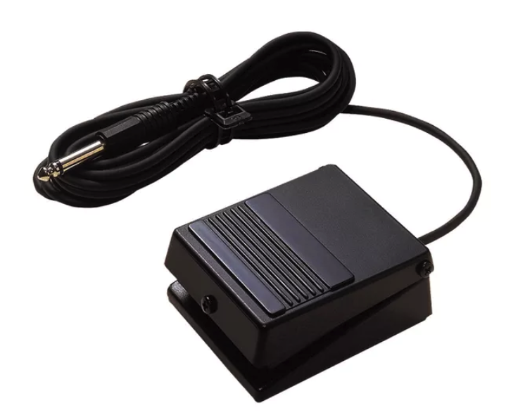
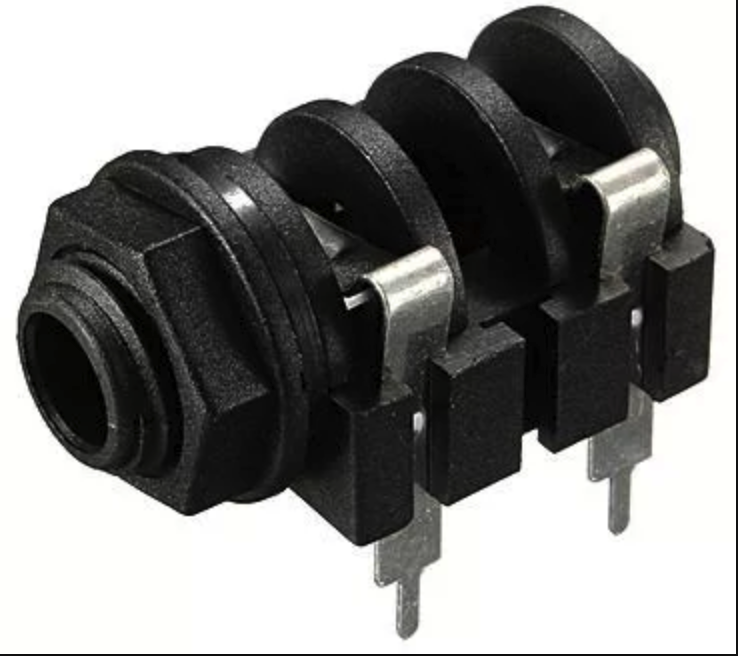
Thank you for making changes to the part that was broken, I have used it and it has worked perfect. I did everything you said, my only issue now is the positioning of the parts for the pcb. The case is a rectangular shape, it will have a panel on the back or side. I will be able to thread the wires through to the jacks because of the holes in the casing for each foot pedal. This is what the pedal will look like, this will give you some sort of idea. Chewie original circuit.fzz (125.1 KB)
Are the jacks going to connect to the pcb via wires? If so you can save pcb space by replacing the current jack part with 2 pin headers (which take much less space.) If they are mounted on the pcb I can’t see how that will work mechanically, the jacks will be parallel to the surface. The bottom row could work, but the two in the middle of the panel will not. This is something that you need to plan out before finalizing the layout of the parts on the board, you need to know how you are going to make it work mechanically before you cut (or even layout) the board. I’d actually suggest that you build the enclosure before you do the final pcb layout, so you know what the pcb needs to look like mechanically before you lay out the board. As I looked at your latest drawing, I saw we have both missed a couple of things. The mega will presumably be powered via a wall wart connected to the coax power jack (aka vin). The mega will then provide 5V for the optocoupler and the circuitry (but at present neither +5V nor ground are connected on the mega). Now there needs to be a different 5V supply (with much higher current than the mega can provide I expect) that supplies the two neo pixels. There isn’t a generic 5V power supply available in core parts (although there probably is one on the web somewhere) so in the modified sketch below I deleted one 1000uf Capacitor (as you only need one of perhaps higher capacitance for both neo pixels) and used a dangling wire in breadboard to indicate the neo pixel power source (that needs to be replaced with whatever will power the neo pixels). You also need to consider that power supply in the mechanical design for the case. You probably want to use numbers (as I have in this sketch, for me your Chewie original circuit.fzz above is saved as Chewie original circuit2.fzz to differentiate it from the previous versions with the same name and thus this new one is Chewie original circuit3.fzz. That way you can keep copies of earlier sketches to go back to when you make a mistake. In any case here is a new version of your last sketch with the power wiring changed in a fairly ugly manner :-).
The pedals are going to connect to the jacks. I did want to mount them onto the pcb, so they are secure. Because they are quite loose on my breadboard. Any slight movement can disconnect them. I understand that you say I need to build my enclosure first, I do really. I just want to get this pcb somewhere close before I make them. I have an idea how it will work in my head. I noticed that the +5V and the ground wasn’t connected on one of the earlier sketches but completely forgot to connected it. My plan was to use a wall wart to power everything. What other way can I power the neo pixels? These are the pedals I am using and also the jack I am using.
The issue here is that changes to one thing affect the other, so you want to have something like perhaps a mock up in cardboard of the enclosure that isn’t a huge cost or amount of work that you can change easily and cheaply (enclosures are typically expensive if you make a mistake) along with a cardboard mock up. print a copy of one side of the pcb layout (to get the position of the mounting holes), tape it to a piece of cardboard or a thin sheet of rigid styrofoam and poke the components in to the pads on the paper layout to mount the components. That gives you an easy (and changeable) version of your pcb and verifies that the components will actually fit on the board in real life (both useful things). You will likely have to iterate around this loop (enclosure mechanics, board layout) several times to get a working design. For instance its possible that you will do an enclosure and a pcb layout then discover that there isn’t enough room on the pcb to route the traces, meaning you need to move components which affects the enclosure design. It is much better to get it right with a cheap mock up in cardboard than cut an expensive board on ly to discover it doesn’t work and have to redo it. I’d be inclined to start with the enclosure mock up then see if you can place the components and route the pcb to match that design (if not you need to change the enclosure design).
That was a potentially fatal error. If I hadn’t remembered to look for a source of +5V (because Fritzing will happily let me add VCC tags in schematic without a source of power to drive them) you would have routed the board and it would show routing complete but not actually work, because it didn’t have a connection to +5V anywhere. You should verify every wire on your physical breadboard is also in the Fritzing breadboard view as I expect those two wires are on your physical breadboard (because it works) but not in Fritzing (which is a problem). Note that you need to make this change in all your sketches as well so if you end up using one of the other ones you don’t hit the same error and not catch it before you buy a board.
Have you connected the neo pixels to your breadboard set up and run them? It is possible (but I think unlikely, although I’ve never actually used neo pixels) that they take less current than I expect. I do know from articles from people using them they have ugly power draw issues due to how they work. The issue is the 5V connection from the mega can only supply a limited amount of current (I can’t see a spec for 5V but the 3.3V is limited to 50ma, to be powered from USB the 5V line has to be less than .5 A and I expect the output pin can only supply 50 ma as well). I expect the neopixels will take a lot more current than that (possibly several amps) but you may have few enough of them that they won’t need that much. From the 2 1000uf capacitors, someone expected the neo pixels to draw a large amount of current I think (whether they are correct or not is another matter .)You would need to check the specs for the neo pixels you use to see what their maximum current draw is (and I would size the power supply to the maximum current draw!). If the mega can’t supply the 5V to the neo pixels (which I think is likely) then you need to be able to supply the 5V for the neo pixels some other way. A 12V multi amp (sized to match the neo pixel draw) wall wart will supply the 7 to 12V the mega needs and one of the ebay buck power modules (there are fritzing parts for several in parts submit, but I don’t think in core) will reduce the 12V from the wall wart down to the regulated 5V the neo pixels need. From your point of view that means you probably need to add a coax power jack to connect to the wall wart in Fritzing, which is the source of 12V. A 1n4004 diode and a 100UF capacitor then connect 12V to the Vin pin on the mega (this should be able to power the mega from what I see in the mega reference schematic and the diode and cap isolate the mega from 12V voltage fluctuations caused by the neo pixels). This forum thread:
has pointers to 2 such converters (limited to 2 Amp output I think) that have fritzing parts and are available on ebay and others. You would need to verify that 2A is enough current to run the neo pixels first (and find a higher current model if not). Now the 12V input from the coax jack goes to the input side of the buck module, and the output side (which you need to adjust to output 5V before connecting the neo pixels!) provide the +5V to the neo pixels (with probably just 1 1000uf capacitor). Assuming you can use one of these converters a 12V 1A wall wart should be fine (cheap and common) as that would provide about 3A at 5V via the buck module. You should modify both your physical breadboard and the Fritzing sketch to add these things and then test the physical breadboard to make sure everything still works correctly. Then you should be ready to do the component layout in pcb (as there are now a few more parts) and see how you can make the enclosure once you have everything you will finally need connected up.
Hello, thank you for your reply. And sorry for replying late, I have had a busy week. Anyway I have been working away on this project. I’ve been working on the casing so hopefully that might be made really soon. I’ve also been trying to work on the PCB. I have been moving a few things around and also changing pins 13 and 46. But I am still having issues, I can get the PCB to fully route when using auto route but obviously it makes a mess with the traces. But the main problem is traces and parts getting in the way of each other. Could anyone help me out? I’m really been struggling. I’ve also been looking at other software too. Chewie original circuit.fzz (129.3 KB)
I know auto routing is a bad idea, I have tried moving the pins about for the pcb layout. I have moved them on BB view then corrected the schematic. The schematic isn’t the tidiest but I didn’t have much time. Would someone take a look please. Not sure if I have broken the schematic view thanksChewie original circuit edit.fzz (136.2 KB)
I can’t fix it because i don’t know about electronics, all i know is when i see something strange in FZ.
I see a ratsnest in BB on the Mega. I think you must have forced a connection in SCH and it thinks you now need that connection, or one of the wires in BB isn’t actually connected so FZ is putting one in.
The junctions aren’t text book, so it’s hard to know what you intended. If you look at the R27 there is a big junction on pin i but a small ones on the wires below. Big junctions signify a double or more connection, where as a small one is just a bend in the trace, and because there is on big junctions on the traces below you are never sure what is actually connected. I think I mentioned it before, but you run a trace from a part pin to a bendpoint, or you hold ALT and click on a bendpoint and make a trace to the part pin. Then grab the big junction and move it around and check all the traces stay connected and move with it - 4 junctions are a bit weird and don’t all move -.
Other rules is that you always have a black trace between parts, ie no part pin to part pin, and no part pins sitting on traces, eg R28. This like that can lead to thinking you have a connection when you don’t.
Other than those fine points it looks pretty neat.
If you want to switch to other EDAs they don’t have a BB view, which is one less headache to worry about, and they force you to do the whole SCH first and export it into PCB view, which has less chance of errors, if the SCH is correct, because the views aren’t connected.
Yes there is an error in schematic, probably caused by moving wires around which can cause (as it appears to have in this case) unwanted connections. The initial state of the sketch is BB has 2 connections to route (indicating an error in schematic as bb should be correctly routed now), schematic is routed and pcb has 4 nets routed (but no apparent traces which may be a problem later!). Looking at schematic the problem is pretty easy to see: several of the mega’s pins are shorted together. In most cases pins on a micro won’t connect to other pins on a micro. To fix this, in schematic view delete all the wires that connect to R27, mega pin D46 and mega pin D13. That leaves the correct connections shown by rats nest lines ready to connect again and in bb view routing is complete. This sketch has bb view partly corrected (details below) and the offending wires deleted leaving the rats nest lines:
In breadboard there is a cosmetic issue: The LEDs have resistors under the LED where they can’t easily be seen (they appear to be connected correctly though). I would change the layout to make the resistors obvious (which I have done for the CLEARL and BNKL LEDs in this sketch, the other 4 need to be done the same but I was too lazy to do them ). In this sketch the rats nest lines in schematic have been properly routed so the sketch should now be correct (although as noted 4 nets in pcb think they are already routed which may be a problem later).
I would suggest that your next step in this project should be to adjust breadboard to finalize the power supply details (a 12V wall wart and a buck converter for the 5V fro the neo pixels as discussed above) so you are working on what will be (we hope anyway!) the final layout.
edit: I downloaded Chewie original circuit.fzz above and autorouted it. While autorouting is (as in this case) ugly, it can provide a useful starting point to move the traces in to a more sensible order (as long as you are careful). It looks like this layout is wide enough that autorouting will at least complete, so if you add the barrel jack and buck converter to finalize power you could then work on moving components around to improve pcb routing. If your mega pins are movable, I’d suggest looking at pcb to see which traces are hard to route and if changing to a different pin on the mega (if that is possible) will make routing easier (when making changes you need to disconnect all wires to all the pins you are changing in all three views before starting to make the changes though.)
 ). In this sketch the rats nest lines in schematic have been properly routed so the sketch should now be correct (although as noted 4 nets in pcb think they are already routed which may be a problem later).