Cheap RFID reader for 125 kHz tags.
I ask for lenience, this is my first fritzing part.
RDM6300.fzpz (21.2 KB)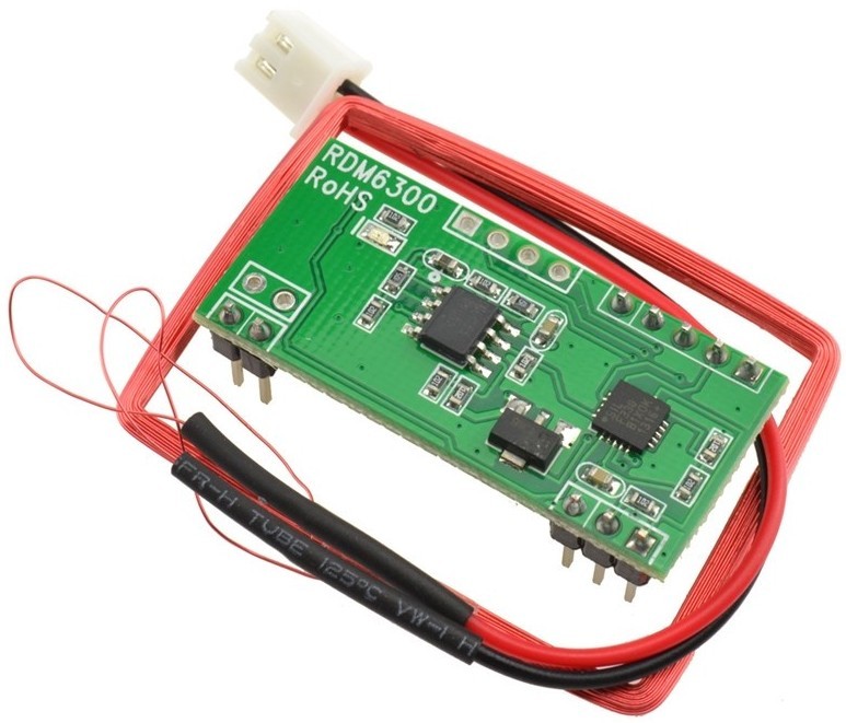
RDM6300-ANT.fzpz (7.0 KB)
Cheap RFID reader for 125 kHz tags.
I ask for lenience, this is my first fritzing part.
RDM6300.fzpz (21.2 KB)Nobody will have a go at you for making parts, in fact we applaud you, but we will tell you what we see because we want people to get better.
for - RDM6300.fzpz (21.2 KB)
In the PCB you need to delete the black rings in the pads "path12631"
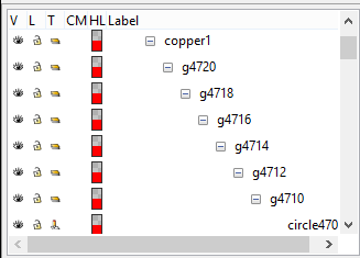
You need a group called “silkscreen” with a black rectangle outlining the size of the part.
Level with the “silkscreen” group you need a “copper1” group where you put “copper0” inside. You need copper0(bottom copper) inside copper1(top copper) for 2 layer boards.
You can export the gerbers and load them into free Gerbv to see what production will be like.
Again by and large an excellent part. As Old_Grey noted the board needs some work on copper0/copper1 and silkscreen, I chose to have a bash at the antenna part.Below is an fzz file with your original antenna and my modified version which consists of the following changes:
pcb.svg: added a copper0 group and silkscreen. Changed the rectangles used as the pads to circles (Fritzing won’t drill the hole in a rectangle I don’t think, it certainly isn’t in this case).
Schematic.svg added a connetor7 terminal (which didn’t exist) and moved connector6 terminal up so that it is in the correct position on the end of the pin. Made the containing rectangle a bit bigger and aligned it to the .1 grid lines (not really necessary but neater) ungrouped everything and regrouped it (without the many many groups Inkscape loves to add) and removed most translates. I think one of the translates was causing the grid misalignment.
breadboard.svg was good as is (nice job!). The only visible change is the red dot in the center of the connector, and that is caused by changing the connector type from female to male in the fpz file. Again all svgs were edited to remove the px on font sizes after being edited with Inkscape.
fpz file: added connector6terminal and connector7terminal (both missing) to the schematic connections, changed both connector types from female (used to mark breadboard pins, not to indicate the type of connector!) to male. The results of all of this are visible in the fzz file. To test this (and both parts I make and ones like this that I’m reviewing) I create connectors of the appropriate length (2 in this case) from core and use them to make connections (at an angle) to the new part. This shows up errors such as lack of a terminal definition in schematic (you will note the original part makes the connection to the middle of the pin, which is the default it there isn’t a terminal correctly defined). The new part connects to the end of the pin as is desirable. The part is also aligned to the .1 grid where the original is offset by about .05 in from the grid. In pcb view you see that I can make connections on both sides of the board to my part, but only on one layer (due to no copper0) on the original. More importantly if you create a gerber file from the pcb by selecting
file->export->for production => extended gerber and view the gerber with a gerber viewer such as gerbv, you will find while the square pad appears in one copper layer, there isn’t a drill hole in the pad (I assume because it isn’t the required circle for Fritzing to calculate the hole size). The new part has the needed holes. From the fzz file below you can export a copy of my modified part from the temp bin by right clicking it and selecting export part to get a copy of the files to see that changes. Feel free to ask about anything that is unclear, as we would like to encourage everybody to make more parts  .
.
RDM6300-ANT.fzz (17.6 KB)
Peter
I apologize for my English. It is very weak and so it may happen that I understand something wrong …
I thank you for valuable and comprehensive comments. I will remember it when I’m going to do something like this in the future.
However, I am a little confused. It sounds to me like you did some corrections. But where is it? Where can I download the modified files (I do not mean the antenna) ?
Thanks, Lubos.
I did some corrections on the antenna part which are in the post above, in the RDM6300-ANT.fzz file, the same changes (adding copper0 and silk screen at least) still need to be done on the RDM6300.fzpz file but I haven’t done them (I’ll let you practice your skills on that one, feel free to ask for help if you can’t figure out how to do it). I also made some corrections to your USB converter module that are in USB converter CP2102_mod.fzpz in the post for that module which are similar to the ones needed here. Those two examples should show you what you need to do to fix up the RDM6300.fzpz file to be correct.
Peter
This is the format for groups, silkscreen and copper1(top layer), with copper0(bottom layer) inside copper1.
Simple resistor xml for the svg
https://scontent.fsyd4-1.fna.fbcdn.net/v/t1.0-9/18836073_10211003056686152_3115911194126915049_n.jpg?oh=b57997b35b017ef6d07233a3aab5f877&oe=59A67C29
Okay, so it was really a misunderstanding caused by my miserable English.
Well, I will improve it. I also thank you for the new valuable tips and guides.
Lubos
I hope I have not missed something or forgot something.
Here is the corrected version: RDM6300.fzpz (20.6 KB)
Lubos
Your written english is certainly fine, I suspect some of your problem may be that we tend to use North American slang and concepts that don’t translate well (or at least so I was told by a translator who had to translate a technical presentation I gave in South America some years ago). So if you don’t understand, just tell us so and get us to try to explain more clearly. That said your latest one is pretty good, only a couple of issues in the pcb svg:
hole size = pad diameter - stroke-width*2
or
hole size = pad radius - stroke-width
(both these values are available in xml editor making them easy to find). However in this case I can’t figure out what units Inkscape is using in xml editor (if anyone knows, please tell me!). None of mm, in, or px work out, so I cheated and did a copy/paste of one circular pad from a .1 connector from another pcb svg and pasted it in to our pcb svg. I then moved it in to copper0 (by indent node a couple of times) and copied its radius and stroke width values (r 2.0880001 stroke-width:1.44000006) from xml editor in whatever units Inkscape is using here before deleting it. Then in xml editor I changed the size of all the circles to those two values (and changed the id of circle14551 to connector57pad as connector57pad is currently the rectangle rather than the circle, Fritzing appears to correctly select the circle to set the hole size, but this change is more correct). Then I increased the size (by dragging the edges) of the rectangles till they again cover the circular pad and we are done. So create a sketch with the new part and add some connectors for testing and route all three views then save it. Now in pcb view select file->export->for production->extended gerber and produce the gerbers. First we use notepad (or any editor) to verify our hole size by editing Untitled Sketch_drill.txt which gets:
; NON-PLATED HOLES START AT T1
; THROUGH (PLATED) HOLES START AT T100
M48
INCH
T100C0.038000
%
T100
X019875Y018362
X009898Y007486
…
X016889Y018333
From which we see all of our holes are plated through (as desired) and set to .038 diameter. (the T100C0.038000 line which indicates the drill label is T100 and size is .038 inches as we wanted). Now using gerbv (or any other gerber viewer) to open the files
Untitled Sketch_copperBottom.gbl
Untitled Sketch_copperTop.gtl
Untitled Sketch_silkTop.gto
Untitled Sketch_drill.txt
which gets us the bottom/ top/ top silkscreen / drill layers and we see that there are pads with appropriate holes and traces matching what we saw in pcb view in fritzing ready to be shipped to a pcb house and cut to a pcb. I also see I’m a little to close on silkscreen between the board outline and the square pads on the top. Note the small indent in the board outline on the top two square pads. That probably means the top line on silkscreen needs to move up a bit. But over all you should now be away and ready to make more good parts ![]() . Nice job you have caught on much faster than I did. The modified part can be exported from the temp parts bin in the fzz file below.
. Nice job you have caught on much faster than I did. The modified part can be exported from the temp parts bin in the fzz file below.
RDM6300_1.fzz (29.6 KB)
Peter
What to say. So much work was still needed to be done …
It is difficult for me to read such a long text and understand it. Perhaps I did.
I’ve reopened my original svg file using Inkscape and yes, I can see that there is no upper contour line there. This is especially good to see in “Icon view”.
This really looks like an Inkscape bug.
Is there some file (created with Inkscape from the scratch) that can be used to import into the Fritzing program (and does not require so many additional edits)?
In fact, I mean, of course, a set of three files (for breadboard, PCB and schematic).
Because the template that comes from the Fritzing export is not 100% OK (at least I think it).
This would be very useful, there would be seen the necessary structure of objects (silkscreen, copper1, copper0, parts, pad size and so on). The structure should be as simple as possible, with the minimum number of nested layers. I was almost shocked when I saw the expanded structure of objects of the PCB file …
As part of such a template, of course, a description of the necessary modifications that need to be done with a plain text editor (such as removing “px” units) would of course be required.
I think it would make it easier for beginners and it would also make it easier for you to work on correcting their work.
Luboš
I’m impressed that you did as well as you did on your first part! Making parts is unfortuntaly complex, and it doesn’t help that it is poorly documented at present (although we are trying to change that). The first one of these describes (with later modifications and more yet to be done!) how I made my first very simple part. Things like editing for the px ending are in there. I’m working (slowly though ![]() ) on a python script that will read either an svg or preferably the fpz file and correct a few things that Inkscape does that Fritzing doesn’t support (px on font size, style command replaced with inline xml) and checks for errors such as missing layers and missing terminal connectors in the svgs that are specified in th fpz (and changing legacy silkscreen color of white to black, although that one is a Fritzing change) but I’m not finished yet (and then I have to document it
) on a python script that will read either an svg or preferably the fpz file and correct a few things that Inkscape does that Fritzing doesn’t support (px on font size, style command replaced with inline xml) and checks for errors such as missing layers and missing terminal connectors in the svgs that are specified in th fpz (and changing legacy silkscreen color of white to black, although that one is a Fritzing change) but I’m not finished yet (and then I have to document it ![]() ). Here is a pointer to the latest parts tutorials such as they are (you may already have seen them though):
). Here is a pointer to the latest parts tutorials such as they are (you may already have seen them though):
Yes, at least sort of, I usually start with a generic IC from the core parts bin and change it to have same (or more) number of pins I need for the new part and change the metadata with parts editor (because its a little easier than with a text editor) then export the part. Now I have the correctly formatted and laid out files to edit to do what I want. I may still need to add or remove pins but at least the basic layout is there. As well the part is correctly registered with the parts data base which needs to happen even if I was to start from a new file.
This one unfortunatly is an Inkscape feature. Even if you start out with minimal groups as you edit it with Inkscape it adds extra groups and transform/translate commands (which I dislike). The only cure I know of is after finishing the editing in Inkscape is ungroup all the groups and remake only the groups that need to be there (although you then need to know what groups need to be there and there order again, but that comes with experience). That removes both the groups and the transform translate commands but is extra work (and the svg will work without doing it).
Peter
I think it is a Fritzing thing that adds groups when a part is exported.
Ah! Learn something new every day! Thanks.
Peter
I used to make parts assembling the svg and the ,fzp externally before I uploaded it so it wouldn’t do that, but then I gave up and just lived with the groups because it was easier to assemble them with FZ edit.
I never actually checked when it added the groups, so it might be the import.