Hello people,
I have a problem with my board. I want to get my board fabricated but when I uploaded my sketch on www.aisler.net, a pad (not really, it is a region where there is no solder mask and the copper is exposed) appears in the board viewer and in the stencil viewer. The pad is not present in the sketch. I viewed the board in different gerber viewers of different PCB manufacturers but the pad is still there. I have attached a few pictures.
Steps I took that resulted in the problem:
I don’t know. I just designed the board as I have done before many times without any problems.
What I expected should have happened instead:
…
My version of Fritzing and my operating system:
I am running the latest version of fritzing on Windows 10.
Did you upload the Fritzing sketch to Aisler or did you export the Gerber files and then upload a zip of them? If you uploaded the sketch could you try exporting the gerbers and zipping them and uploading them to Aisler to see if it is a problem on there end when they try and convert it from a sketch. If it still appears could you upload your custom part here so we can have a look at the part to see if there is something in the custom part that is causing the problem.
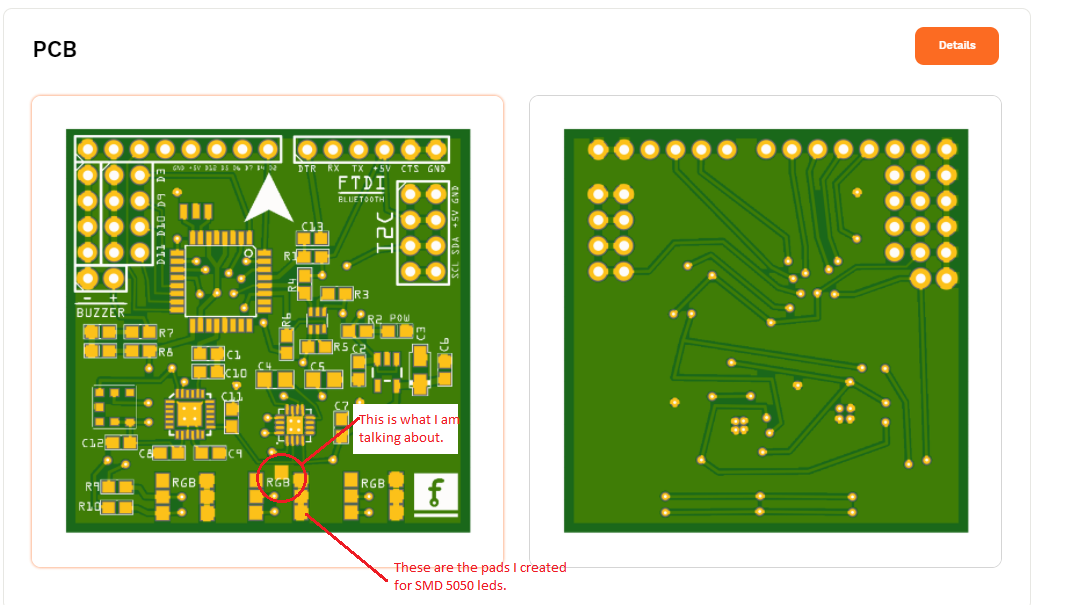
I uploaded the sketch to Aisler. I uploaded the .rar gerber files to www.jlcpcb.com and on www.pcbway.com with the same problem. I did not create any custom parts. I just created some pads and placed them in a way so that I can solder a 5050 led on them.
I suggest you check your PCB design file again. Perhaps this is some small flaws you did not find.
So the emergence of the pad is independent? Does it affect the circuit connection?
Believe me, I have checked my sketch a lot off times. With all kinds of gerber viewers, I see the pad. No, It does not affect the circuit, but this pad might be a problem while soldering using solder paste and hot air gun.
Oh, I believe it.
I mean you can check, your circuit diagram in PCB design software, is there a separate pad that does not have a connection?
If it is not, I really do not understand where it will go wrong
Since you don’t want to supply the sketch people can’t work on it, so your best bet is to do it all again using your old sketch as a guide - it doesn’t take long if you have both side by side -, and ask people to make parts rather than have floating pads all over the place making up footprints.