Question on caps

Hi. I’ve checked the tutorials and parts help, but am slightly confused.

Most of the caps have a TON of variations, but I can’t relate those to common parts sites, such as Mouser. For example, I’m trying to use a 220uf Aluminum cap with say 3.5mm lead spacing. That seems fairly straight forward.

Yet, when I do a search, and drag a cap on the schematic, it has variants like panasonic_c, _d, _e, _g and of course a note I should check the hole spacing. Ok, I got that - but how? What do these other package and variants represent? Panasonic’s own data sheets don’t seem to have lists of these variants.

It’s like I need a rosetta stone :slight_smile:

I know it’s not a huge deal, these are common parts, but I’d like to be able to build a proper BOM.

Thanks, hope this isn’t too much of a n00b question.

== John ==

In general caps are generic. Once you drag it on to the sketch, then Inspector (lower right pane) will let you select things like value, voltage, and package. From the 3.5mm I’m guessing the cap is smd because that isn’t a standard through hole spacing. So you need to know what package it is 0405, 605, 0807 to get the correct footprint. Then you can either look at it in pcb or better, file->export->for p[roduction->gerber as a gerber (which is what the fab house will make the board from) and check there what the spacing is. For the bom, set the part number field in inspector to the correct part number.

Peter

Sure, I get that, but you mention “you need to know what package it is” … where do you get that info???

I’m looking at the data sheet and it’s not there.

I’m asking specifically what is "panasonic_c, panasonic_d, etc.

Someone coded that into the part, but without knowing what that package consists of, it’s hard to know which one to pick, right?

This is through hole, btw; http://www.mouser.com/ProductDetail/Panasonic/EEU-EB1E221S/?qs=sGAEpiMZZMtZ1n0r9vR22RyzzjEKRzqKf0an4qUGcE0%3D

So these are specific Panasonic electrolytic SMD 1010, at least that is what the PCB view shows.

I think you are working backwards from the specific part when you should be picking a generic cap from the CORE bin. Pick a electrolytic from the CORE bin and adjust it to what you want in the Inspector. Pick it in the PCB view so you see the footprint you are getting.

I’d agree with Old_Grey here, most Fritizng parts are generic unless they are for one specific device (certainly caps are generic because there are so many of them). The data sheet for most parts will have the package and usually a recommended pcb footpriint.The 3.5mm lead spacing listed on the Mouser page is wrong, if you look at the actual data sheet for the caps by clicking on the pdf data sheet, the spacing is the standard 2.5mm ,5mm, or 7.5m (i.e. .1 in, .2 in .3 in as selectable in Inspector). As far as I can see the 3.5 mm is the spacing between the hole on the tape and the capacitor lead and has nothing to do with the lead spacing. You should always check the actual manufacturer’s data sheet for the part.

Peter

Thanks. My more general point was, how do you know what these are? I DID check the generic parts bin - I used the ‘search’ box and those six caps popped up. Oddly, they mention Sparkfun, but I did try the search function as there are a ton of parts.

I see your point, I should navigate manually to the core bin - thank you! That helps.

Now, you’re going to laugh - I skimmed the ‘core’ parts but didn’t see a 220uF cap and saw no way to edit the part or lead spacing. doh there is a .22mF cap. lolz.

Honestly, I’m just working backwards - I’m building a circuit board for a friend, and just trying to find what parts Frizing has that he can then order, not necessarily trying to fit a specific part to Fritzing. For those kinds of activities, I’ve already edited parts. It just seemed to me for passive’s I should be able to pick standard stuff out of the bin.

My question really was just “how are you supposed to know?” In the capacitor part there was no key to the different sizes. If I’m expected to place a sample, go to the PCB view, examine the board, and try to figure out what I got … EACH PART I PLACE, this is going to be a real hassle, except possibly for throwing together some Arduino projects.

I tried Eagle, but I thought Fritzing was easier to use.

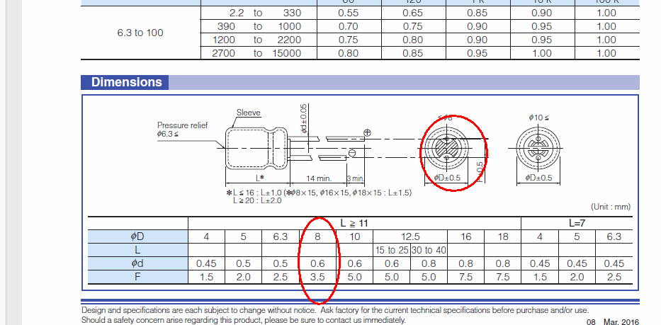
Regarding the ‘standard’ lead spacing, honestly, that’s the kind of stuff I don’t know; I’m an EE but haven’t worked in the industry in a while (into software now) so off the type of my head don’t know what is “Standard”. SO I did check the data sheet :slight_smile: on page 12, caps with a diameter of 8 have a spacing of 3.5.

Then, the 220uF, 25V cap:

I’m a n00b and can’t put two images - point is the 220uf cap at 25V is a 8x11 cap - thus the 3.5.

Still, it’s through hole, so even if I source a 3.5mm it’ll solder fine with 5mm.

Thanks for the advice, I appreciate it!

== John ==

I will admit that I often get tripped up trying to change a part in the parts bin. That doesn’t work, you need to drag the part in to a sketch to be able to change it in Inspector. In this case the forth icon in in the top line of the core bin is a generic electrolytic capacitor and dragging it in to the sketch then lets you change the lead spacing and values. Search is a double edged sword, it has an odd view of search terms. I generally get a whole bunch of stuff in no way related to what I’m searching for and have to dig through unrelated output (sometimes large amounts of it) for what I want. That is probably somewhat because many parts are user supplied and have user supplied tags which is I think what the search function is using.

Peter

Pull the part on to the page, and if the value isn’t in the Inspector drop-down box just type it in. There is some foibles in FZ so you have to type in numbers behind the 1st number and go back delete the first number.

The proper way to design circuits is draw out the design with values.
Build a prototype and adjust values until it works.
Now with the final values do a parametric search in maybe Digikey for what parts you can actually buy, and select one that suits your criteria. It might be price or physical size.
THEN look in FZ for a footprint that matches the part you are going to buy. PCB view is supposed to be accurate engineering footprint drawing, because this is where you organise the physical parts to fit on a PCB in the real world.

You are kind-of working backward choosing a part in FZ and seeing if it exists in the real world, because some parts in FZ might not exist anymore.

If I want a specific part I will do a search, and pull all of them into a new sketch looking for the correct footprint. I don’t care if there are 100 results I will go through all of them, but you can get an idea of the footprint before hand by clicking on it and checking the PCB icon in Inspector.

Thanks old_grey - I did discover that. I’m a n00b so I thought maybe you had to pick a value that was there (and as I mentioned, I wasn’t thinking through my SI units … 220u vs. .22m.

I have a circuit that’s already drawn out, and my brother prototyped it. He’s now asking for a circuit board.

I have to admit I did it slightly differently, I looked at FZ for a footprint for a part I could buy. My logic was that the parts bin didn’t seem THAT big, so I figured it would be easier to use a part you COULD get, instead of looking for a FZ part that I’d chosen (I’m not doing the sourcing anyway, my brother is).

I get your point, I’ll do that in the future. Thanks for the advice.

This part though:

If I want a specific part I will do a search, and pull all of them into a new sketch looking for the correct footprint. I don’t care if there are 100 results I will go through all of them, but you can get an idea of the footprint before hand by clicking on it and checking the PCB icon in Inspector.

Got it, although that seems kind of time consuming - it would be great if FZ had an option that would at least show you the diagram. I checked AutoTrax DEX and it does that (even in 3D) which does make it a little easier to find that part that matches that part.

You guys, thank you so much for answering my silly n00b questions. Now to go order that part with 3.5m leads and see if it exists :slight_smile:

== John ==

It does have a preview, it’s just that it’s small. Just hover the cursor over the part in the bin and the 3 views are displayed in the Inspector in icons. Another FZ foible, some PCB parts have been made with white silkscreen so the outline doesn’t show on the white icon.

FZ is a bit complicated when you make parts because it has a very graphic intensive breadboard view, something the others don’t, so if you are not using that you might like a easier EDA. I like FZ because it looks modern, where as the others look like crude and simplistic stick drawings, and if you do go to a 3D CAD style EDA the drawing is just as intense when you make parts.