If you are good a puzzles you can weave traces around the back of stuff.
https://scontent.fsyd4-1.fna.fbcdn.net/v/t31.0-8/19390605_10211177024435237_5358132903310226007_o.jpg?oh=be926327360d1a51850b4b9544386b70&oe=59E6181A
Peter and Old Grey -
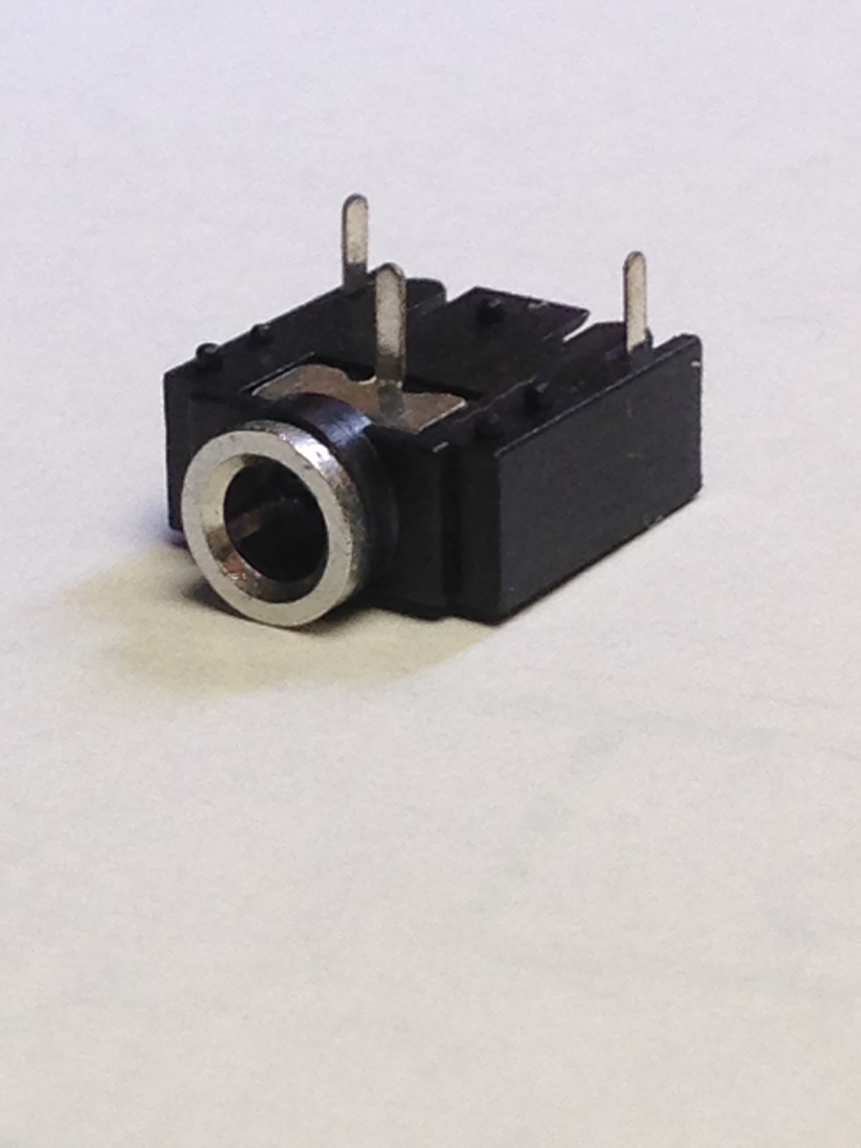
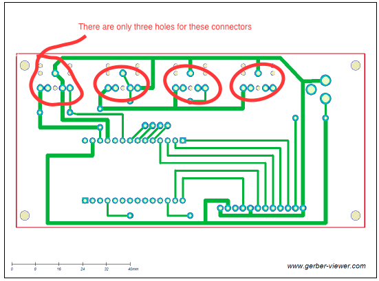
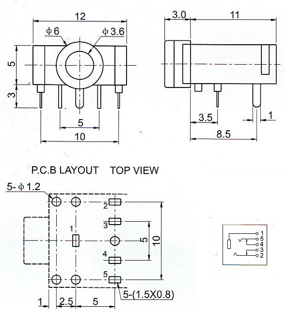
Thanks again for the input. I have attached two files for review. One is the actual stereo jack plug showing the three pins and reinforcing legs that relate to the PCB. The question of the additional two pins that show up in the PCB trace which are not really there bothers me. The preferred trace would not have a hole where there is not a pin. Can I easily delete the unneeded hole in the “stereo jack”, or does it really make a difference if the trace has a hole in it? I can think of several ways to create the same pattern … but that would involve three copper pad holes (or “vias”) in the proper spacing as well as 5 drill holes in the proper size and spacing as well.
As for the power connnector … the one I am using is a part from Adafruit or Sparkfun … not sure which, and the legs do not seem to require a hole any larger than the 1.2mm hole that is standard on the Adafruit perma proto boards. I can not tell what the size of the hole and ring are using the default power connector in the core parts database, but it visually seems much larger. For that matter, as I understand more of the process, I do not know what the default hole and ring size for the “jumper pads”
 are. Perhaps either of you know or could explain how I can determine that. The “vias” default is 0.4 mm hole or 0.9 mm for “home etched”.
Peter -
If I understand the suggestion for the “bypass” capacitors on the LCD board, it is to minimize “noise” perhaps created from the AC conversion to DC at the power connector. Since the MKR1000 has capacitors in place (I assume) … the need to add them on the LCD board is just extra caution, or am I not clearly understanding the need for them? I have not had any formal training in electrical theory or engineering … I am just a competent “handyman” who likes to tinker. I appreciate the challenge to understand when and when not to include components in my projects. Every time I try something new, I learn something.
I am attaching two jpgs for review. Thanks again for the wonderful support and advice.
Old Grey and Peter … and others
After reading some other posts and seeing the Parts Editor video from Old Grey … I thought I would try to edit the Stereo plug I am using in this project. I created a new file in Fritzing, selected one part from core parts (the stereo plug), dragged it onto the PCB layout, then right clicked to open the part to edit. In Parts editor, I went to the PCB view, and see the 5 connections and how to select them … but cannot simply press delete to remove one or two connectors.
I went to the connections tab, and see the ability to remove or change the connections from 5 to 3 by deleting a “ring” or “tip” …
My expectation was that I could simply select the visual graphic of the “circle and ring” and delete it … but that does not seem to work.
My question is how do I edit the graphic elements within that part?
If you are home etching put 0.4mm via on every pad so that it centers the drill very accurately, because if you use the std 0.9mm hole the drill can start off-center. Via size is adjustable in the Inspector. I use toner transfer with that Ebay yellow wax paper etch and tin, and thickness of the copper leaves enough of a step that it centers the drill.
You have to edit the svg to remove the extra pads.
In FZ edit go to PCB/File/Show in Folder, and copy the svg somewhere. Then open it with Inkscape and delete the pads with the XML editor - my video shows you how -, save it and load it back. If you have too much trouble we can make it for you.
I don’t either, but I said “that will be easy, just edit the pcb svg in core and look”. Wrongo! there doesn’t appear to be an svg in the core svg directory (or I don’t know what it is called). I suspect they create the svg on the fly in the code. After some head scratching however I prevailed. I exported you pcb (with jumper) as an svg and then edited that with Inkscape which tells me the pad is .075 inch diameter which likely makes the hole .0.35 (the stroke-width isn’t the standard 20 but 1.44 which is why the probably on the hole size). As to the bypass capacitors indeed all the bypass capacitors are just caution, more needed on the LCD board than the main one, because as you say the CPU will have internal bypass capacitors. The primary issue here is wire length from the source of power (which is going to be longest in the LCD case), as the wires add a small amount of inductance (which resists changes in current by changing the voltage, where a capacitor resists changes in voltage by changing the current). What happens is that if multiple data leads change at the same time and the inputs (which is likely true of the LCD controller) have a high capacitance, when they switch (and depending on how fast they are switching, which with modern logic can be very fast) they draw a lot of current. If the power lead is long and with enough inductance, that will cause a downward power spike on the power line to the LCD (and thus the LCD controller). Without the bypass capacitors the inductance of the wires may temporarily drop the voltage see n at the LCD display. If it drops below about 4 to 4.5V for a 5V supply the LCD controller (or most any other logic chip) may malfunction, and since the LCD controller is essentially a CPU inside, malfunction may be stop working until it is reset. The bypass capacitors near the LCD fix that by resisting the voltage change caused by the increased current draw by supplying the energy required from the energy they have stored in them until the inductance finally allows the voltage to change (which it will quite quickly, just not always quickly enough). Within broad limits (the notable exception being rf which is much more complex, although this isn’t all that easy ![]() ) more bypass capacitors are better. The usual rule of thumb is a .1uf ceramic capacitor close to the power leads of each chip and larger tantalums every 4 or 5 chips. If you don’t use them it will likely work just fine, but its possible that it will work fine %99 of the time but every once in a while the system will hang until you power cycle and reset everything. That is a very hard and frustrating problem to find and fix (and is expensive if you have cut and assembled a bunch of boards and it turn out to need more bypass caps!). As a result I tend to stick extras in.
) more bypass capacitors are better. The usual rule of thumb is a .1uf ceramic capacitor close to the power leads of each chip and larger tantalums every 4 or 5 chips. If you don’t use them it will likely work just fine, but its possible that it will work fine %99 of the time but every once in a while the system will hang until you power cycle and reset everything. That is a very hard and frustrating problem to find and fix (and is expensive if you have cut and assembled a bunch of boards and it turn out to need more bypass caps!). As a result I tend to stick extras in.
Peter
Unfortunatly parts editor is a work in progress and at present can’t make those kind of changes. To do so you would need to save it as a new part (without any changes except maybe to the metadata to explain whats different about your new part) and the edit the svg files with an svg editor such as Inkscape (which I use because it is open source, and is thus what a lot of us use). Old_Grey’s videos explain that too, but if you aren’t familiar with an svg editor (as I wasn’t  ) it has a steep learning curve. I suspect that Sparkfun cloned your jack off the one with bypass switches (which uses the extra pads) and didn’t delete them. While you are welcome to try Inkscape, you may find it easier to use this part that I just edited off the one you have, cleaned it up a bit and deleted the two extra pads.
3.5mm Audio Jack_no_extra_pads.fzpz (7.9 KB)
The pad holes here are 0.051181 (which will likely round up to the standard size of .052). Once you are familiar with parts creation and Inkscape this is a pretty short task, its just getting that experience that hurts (although it is worthwhile if you like Fritzing which I do). If you need changes to the power plug I can do that too if you specify a hole size. Note that the fab houses usually have a list of standard drill sizes. My local fab has this set for free (they have other sizes, but they charge if you use them):
.0197
.0280
.0350 ic pins
.0380 .25 connector posts
.0420 1n4001 diode holes
.0520
.0595
.0860
.1250
.1520
I expect the Fritzing fab has a similar list on their web site somewhere.
Peter
Thank you both … Peter and Old Grey
I have some graphic experience and may want to do some editing of parts in the future. Your library is pretty darn good for the majority of users I imagine!
My intention is to use Fritzing as the PCB fabricator (unless there is an alternative for beginners such as myself)
Old Grey had mentioned [quote=“Old_Grey, post:24, topic:3995”]
I use toner transfer with that Ebay yellow wax paper etch and tin
[/quote]
Is that going to give me the text labels as well? I would then have to drill the holes I am sure.
I am not sure I want to try to drill and etch my own board … for several reasons, such as the silkscreen labels for text, and the exactness required for drilling so many holes with 1mm spacing. Am I wrong in this assumption? If I had a CNC machine, or you know of a modestly priced alternative … I could be persuaded to give it a try. But for now spending $100 US for 3 sets of the 2 boards seems reasonable. Certainly if I were doing larger production, it would be different.
I will post final efforts soon. Let me know what your thoughts are about “self etch” vs. “commercial fabrication”.
Jim
It won’t give you the silkscreen I don’t think, and yes you need to drill the holes. I prefer a fab house which is more expensive but much easier (and you do get silkscreen and potentially plated through holes if you use double sided).
There are alternatives for sure (possibly cheaper) but if you are good with the Fritzing fab price I believe they feed some part of it back to Fritzing to fund development so thats good. I’ve heard some of the folks in here using oshpark who advertise $5 for 10 boards (that is likely for a 1" by 1" board though) and I think some of the chinese suppliers are even cheaper (but with no checking of the boards, what you send them is what you get). I favor ap circuits mostly because they are one province over here in Canada and thus I don’t have to worry about customs. Their usual ad is 2 boards to sides $20US. They also have an online estimator that will give you a quote. The Fritzing fab is in Germany I think and thus depending where you are you may also have to add custom fees. Hopefully some of our folks that make more boards than I do will chip in with an opinion ![]() .
.
Peter
I am also in Canada and looked at AP circuits for boards but their online quote was $1100 and from China with file checking and guaranteed quantity it cost $9.80. And no there are no missing decimals it was really eleven hundred dollars for 10 boards and under ten dollars from China (plus $3 for E-packet shipping that takes less than 2 weeks). They were 98mmx99mm x 0.6mm thick boards with a lot of milling and hundreds of pads, holes, silkscreen on both sides and not just green solder mask but still $1100 is ridiculous plus I would have had to pay tax on that where as the ones from China came in at under the $20 customs limit. So far I haven’t had any bad boards but I have read 1 in 200 fail.
Interesting! Care to share the url of who you are using in China? After all, I may at some point need some boards (I usually use perf board or the ebay one pad per hole fr4 boards as I’m usually only making one and not that complex), plus I expect others will be interested too. Its always better to start with somewhere someone else has had success with.
Peter
I was not sure about sharing links to fab shops because of the relationship between Fritzing and Aisler but since you asked. I have used Elecrow with only minimal problems. No problems with the boards themselves just problems with the way Fritzing does some stuff on my more complicated boards that cause their software issues. When there is an issue they will email you with a cryptic message that is no doubt the result of translation to English from Cantonese at which point you may have to make some small changes. Things like Fritzing tiny silkscreen text is 0.7mm tall and Elecrow wants 0.8mm tall or greater.
Also when you order select registered mail and then in the notes ask them to use E-packet (EUB). It is as fast as DHL but costs almost nothing and rarely gets any customs charges even when above the $20 threshold.
Me either, but I guess we will see ![]() (I grabbed a copy of the url just in case, thanks!). The times I’ve seen a post removed it has been someone obviously just spamming with no relation to Fritzing which isn’t the case here.
(I grabbed a copy of the url just in case, thanks!). The times I’ve seen a post removed it has been someone obviously just spamming with no relation to Fritzing which isn’t the case here.
Peter
I toner transfer the labels as well.
https://www.mediafire.com/convkey/faa1/ci962cii6j21cpp6g.jpg
https://www.mediafire.com/convkey/2a56/lad32icvcl8jomj6g.jpg
You can DIY at home, but it’s a lot of trail and error - took me 1 week and I’m a Mech Eng - and in the end it’s never going to be as good or as easy and getting it made.
As for the power connnector … the one I am using is a part from Adafruit or Sparkfun … not sure which, and the legs do not seem to require a hole any larger than the 1.2mm hole that is standard on the Adafruit perma proto boards.
The blade pins on the audio jacks might be wider than 0.052", someone will have to measure them.
2 Likes
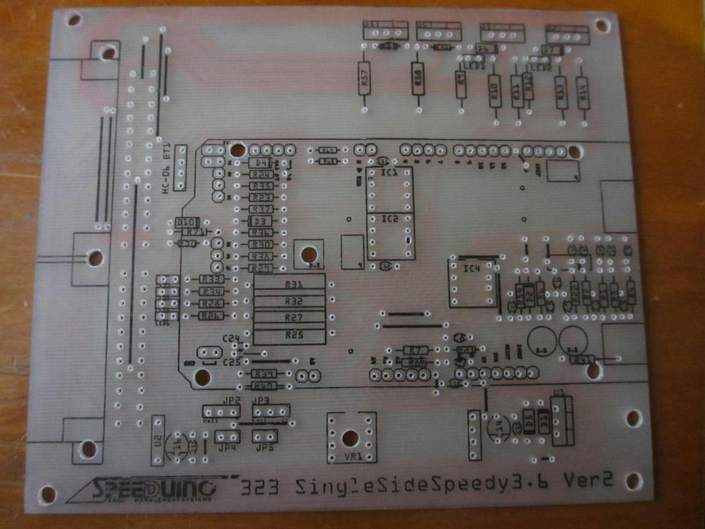
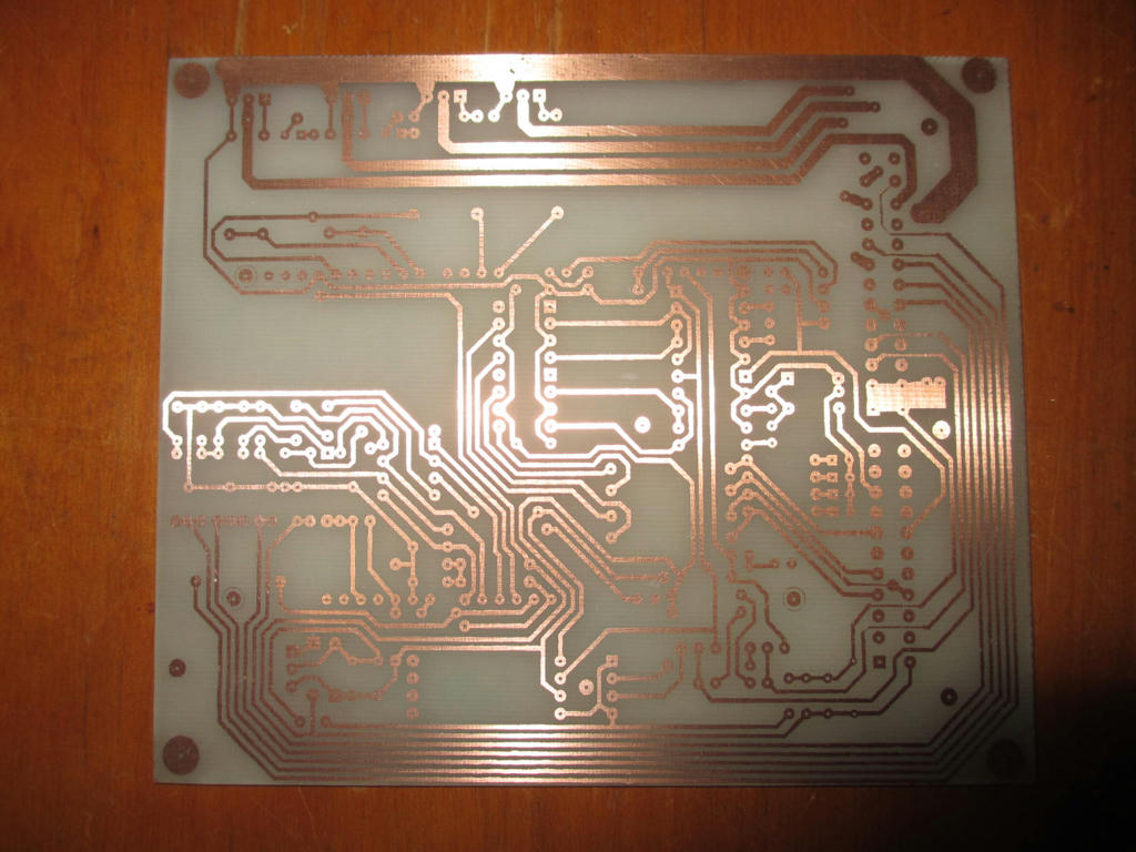
That’s an impressive looking board. If I just saw that without knowing what it was I’d have guessed fab shop. Technology has obviously come a long way since I last tried this 30 years ago or so.
While it is always best to check, it came from a Sparkfun part and I’ve found them to usually be pretty good quality.
Peter
I think this is the one.
http://s2.electrodragon.com/wp-content/uploads/2012/04/3F07-Double-Sound-Channel-3.5-Audio-Jack.jpg
I agree, that is quite an impressive board for self etch. As you said … lots of time and effort.
At this time my learning curve with Inkscape has allowed me to understand stroke and fills … and use the x,y coordinates to verify positions of objects.
However the x,y coordinates seem to relate to the “edge” of an object, rather than the “center” of an object. Is there a setting that I have overlooked, or how can I change the size of the pads for the power connector from 3.5 mm diameter and 0.5 stroke to the desired size of 1.75 mm diameter and 0.35 stroke … while keeping the center location UNCHANGED?
The stereo jack edit was easy … ungroup and delete the two unwanted circles. Then save as a new file name and select from mine parts.
Assuming I’m converting correctly (unfortunatly usually not a good bet though  ) 1.5 mm on the long side which should be 0.059 and the hole in the part is .052. If you have a jack and a vernier caliper, measuring a pin both ways would be a good bet. It is easy to boost the size of the hole a bit in the new part if we need to before boards are made. The mounting holes agree with the data sheet at .0472 (or 1.2mm) so its possible the pin holes are too small. Also even though they aren’t connected, the data sheet shows the 2 pins I removed as being present (which could be a problem if they are there on your parts).
Peter
We are addressing several questions at one time, and I think a short review would help me clear things up.
The default drill holes on an Adafruit perma proto board are 1.4 mm / .047"
The holes on the “stereo-jack-3_5-08780_h.svg” are 1.78mm with a .35mm stroke … leaving a 1.43mm hole.
My SAMPLE of the stereo jack fits just fine in the 1.4mm holes on an Adafruit board. There are only 3 pins. That’s good.
The holes on the “connector_power_pj202ah.svg” are 3.5mm with a .5mm stroke … leaving a 3.0mm hole. That’s too big.
I have successfully edited the stereo jack, but am not sure how to change the hole size in the “power connector” and keep the holes in the SAME CENTER to CENTER location.
The x,y coordinates relate to the edge of the object, not the center.
Comments or thoughts?
Jim
Assuming Inkscape, if you change the radius in xml editor the pad will expand around the current x/y location. The tricky part can be to figure out what units it is using for the radius. When I can’t figure that out I cheat by creating a pad (in the same group where the one I want is so the translates are the same), resize it to what I need and then copy the radius it used there in to the part that I want to expand but stay in the same place. Then I delete the test pad. If someone knows of a better way I too would like to hear of it! I notice in the description in inspector they comment that the PTH (which is the 3mm hole according to the gerbers) is the most reliable and proven footprint. Since I’ve not used it I’m not sure, but the above should let you set the hole size you want. I’d try and find or make a hole of the selected size and try the jack you have (whicn may be different than Sparkfun’s) to make sure it will fit.
Peter
Yes, Inkscape refences from the bottom left of the page to the bottom left of the objects.
What you do is set a grid, you can use offsets, and then use the different snap buttons so that when you move it close it snaps to the correct position.
Yeah, that child of parent group is a pain.