All -
I am trying to make a jumper longer than the default length that is created in the “core parts” jumper selection. There does not appear to be a setting to change the length from what looks like .4". I have seen comments about being able to convert a trace to a jumper, but in my version 0.9.3 running on a Mac, I do not see this option.
Any thoughts would be appreciated. Thanks.
The obvious question would be how to design a PCB without jumpers. Try as I might, I cannot seem to overcome “boxing” myself into a “hole” with some of the connections. Is there a logic or a method of understanding how to layout parts to prevent “illegally” crossed traces?
If I post the file, would anyone be willing to offer suggestions?
Don’t know about the jumper question, although as a work around a one pin connector on each end of the jumper will do. That creates a pad that you can solder a wire to. I’d say post your board at worst no one comments but that is somewhat unlikely there are a number of skilled folks in here.
That is what I have done. I just does not have the “look” of a jumper that makes “following” the PCB layout a easier.
I will post the fzz file just for comments. It is a two board combination … one in a lid with a 16x2 LCD and few LEDs and the mainboard in the bottom of the project box with the power input and sensor connections. I am using 2.5 mm stereo plugs to have remote sensors on three conductor cables about 25’ long.
Not sure if this is the proper way of uploading a file, but if it does not work, perhaps someone may correct me.
Yep the upload worked fine. Ah the joys of single sided boards sometimes jumpers are the only answer on single sided, but in this case I think you can avoid it. Starting from the 2nd from left pin on the top row of the MKR1000 you could route a trace between the pins by the flow leds connector to connect to the tmp 36 connection that currently has the jumper. That probably assumes that the board is being made by a fab house rather than self etched to get the necessary clearance to go between the MKR1000 pins, but even self etching might work. Someone else may also see something I missed as I don’t do boards all that often.
Peter -
Thank you for the very rapid replies … much appreciated.
The jumper you see in place is not really the problem. I have two other jumpers still to be positioned. At this time they are being “created” using single pin headers and I will just plan on soldering in wires later. If you refer to the PCB layout for the main board … they show up as the 4 single pin headers.
Just trying to use jumpers that I can see as a visual reference.
Yes I see your issue. It isn’t possible to tell where the jumpers are supposed to be from the drawing. You could label the pins something like j1-1 and j1-2 (for the two ends of jumper1) and j2-1 and j2-2 for the next one on silkscreen. That would help some but a resizable jumper would be better (but I don’t think is an option currently). The other thing you may be able to do is change I/O port assignments (since the DHT22 seems to be one wire and only needs any port not SPI or I2C) to make routing easier. The temp sensor for instance could go to D13 on the micro without a jumper if that is acceptable (although I suspect it is analog as something appears to want an analog pin, in that case a trace between pins 22 RX and 23 TX would eliminate the jumper. ) and a single jumper would take the dht22 to pin D10 on the micro. That would mean software changes, but may be worth it to save pcb routing.
edit: a late thought, if you need to leave the pins as is, I’d probably move the two connectors under the micro to just above the header on the bottom right (you may need to move the two traces there up a bit to make room). That gives your jumper wire a straight shot between the two pins (if you extend the one on temp sensor in the space available so it is in the same area as the DHT22 one).
edit2: I see several problems (having had a look at the MKR1000 data): first is a simple error, you have a short between 5v and ground on the header on the bottom right. The ground trace on the bottom goes one pin too early (5V rather than ground next to it) according to the labels. Then your sensors all appear to be running on 5V (not 3.3V) and are providing a (probably) 5V input signal to a 3.3V device (which the adafruit description warns against). For safety you either need to run the sensors on 3.3v (if they will (the dht22 will, don’t know about the other 2), or can be replaced with 3.3v versions which is easiest) or provide an input level translator to protect the cpu (more parts on your board). The hall effect sensor is powered from the 5V pin (which is only active when USB is connected), is that correct? I’d expect it to be powered from Vin (5V) on the next pin or from the 3.3V pin (which is currently unused) so that level translation isn’t needed. This will change your pcb routing and may make things either easier or harder .
Don’t know if it was covered because i didn’t read the whole post, but you select the jumper and grab the end and drag the length and position you want.
If you drag a single jumper wire (blue jumper wire) out from core parts bin onto the PCB view then move you mouse to one of its corners (if it was a rectangle) you should see the mouse icon change to a small curved arrow. If you click and drag this new curved arrow cursor you should be able to stretch the jumper and place it on angles etc.
Finally got it, thanks! I think my problem was that I didn’t click on the part to select it, and without that the rotate cursor doesn’t appear. Once I left clicked on the jumper to select it and moved the cursor to the edge of the dotted line enclosing rectangle down where it curves around the pad (but not on the straight section!) indeed the cursor changes to the rotate arrow and I can extend or rotate the jumper. This is exactly what the OP wants to do! Learned another new thing about Fritzing!
The answer to using jumpers does lie in the ability to anchor one starting point … then using the cursor to find the “rotate” corner and click and drag to stretch. Just what I was looking for. Do you all think I still need single header pads at each end of the jumper, or does the jumper create a hole and pad at the end of the trace to which it is attached? Or, simply use a short trace or a bend point and attach the jumper at that point?
I will be using Fritzing’s lab to create the prototype PCB’s. I assume that the lab will have seen this before. Perhaps when I create the files to send, the pads and traces will be easy for me to see.
Peter -
Your comment of the “short” to ground … yes, I saw that last night, and have corrected the problem. The voltages of all the sensors is within the 5 Vdc power supply that I am using in the circuit. I did not feel it was necessary to pull from the VCC at 3.5 Vdc to power the remote sensors. All of the internal IO pins and any LEDs will of course be at the reduced 3.5 Vdc.
Getting ready to send final files to Fritzing. Anyone want to see the last edits?
Thanks again to all three of you for the clear responses … Old Grey, sublimeartistry, and Peter. Your comments seem to be very well respected.
The jumper creates its own pads so you no longer need the connectors. As a final test to make sure all is ok, export the gerber (which is what the fab will use to make the boards) and use a gerber viewer (I use gerbv from the geda project, but there are others and online versions) to look at the gerber output independent of fritzing. What you see on the gerber is what the board will look like, and in rare cases fritzing sometimes makes mistakes (although probably not in this case).
The problem with running the sensors on 5V is that their output that then goes in to the micro is at 5V and the micro inputs are not 5V tolerant (i.e. they are likely to eventually fail if you expose them to more than 3.3.V). As well as noted, the 5V pin running temp is only present if the USB cable is present and powered (which may or may not be a problem in your application, although unless you want the temp to not run if USB is unplugged it would be better to power it from a stable power supply). Note this warning from the adafruit mkr1000 page (I tend to like the adafruit pages for things because they have good advise and data sheets :
“Warning: Unlike most Arduino & Genuino boards, the MKR1000 runs at 3.3V. The maximum voltage that the I/O pins can tolerate is 3.3V. Applying voltages higher than 3.3V to any I/O pin could damage the board. While output to 5V digital devices is possible, bidirectional communication with 5V devices needs proper level shifting.”
In your case the 5V sensors are driving 3.3V inputs and would need level shifting to be safe (in the temp sensor case which looks to be analog in, it is difficult to level shift it, not impossible, just not worth the trouble usually). Sure post the final layout, more eyes are always a good thing before commiting to buy boards .
After you have finished you open the gerbers with Gerbv - free gerb viewer - and you can actually see what the PCB house will see. You can even measure stuff inside it.
I am attaching the Gerber print pattern for review … I think it looks OK, but this is my first attempt. The holes for the “Power Input” seem larger than expected, but the part is a standard from the “Core” library … I think from Sparkfun. Don’t think it will present a problem.
Even the “holes” from inserted parts are properly indicated.
I did correct the wiring for the Vin and Vcc connections, and am including the Fritzing files as well. Thanks for helping me understand that a bit more clearly. Some of the components will still get 5Vdc … specifically the LCD, but that is within specs.
I think that pwr connector has flat pins that require a slot, and last time I tried FZ couldn’t do slots, at least not in the drill.txt file, so the parts has to have big holes because of the large pin widths.
If you are going to a PCB production house you can weave traces around so you could cut 3 jumpers.
You could also delete those 4 single header and connect directly, because currently that are sitting on the jumper ends not connected. It makes the SCH incorrect.
With the warning that I don’t often do boards (and thus you would be best to get one of the other folks here to look this over) here is how I would change your board and why:
remove the 1 pin connectors on the jumpers as redundant.
Set the grid size to .025 from .1 for more room
straighten jumper4 for neatness.
Move the CPU end of jumper4 up a bit to clear the cpu more easily (because I can)
Reroute jumper2 so it is straight
reroute jumper3 so it is straight
make the future now by connecting the future jack live pin to unused i/o pin A4 which can be either analog or digital depending on software. Now a future sensor is a software change.
boost the trace size on ground to 48 mil (because we have room and bigger is better, we want the resistance in the power path to be as low as possible).
boost +5V and 3.3V to 48mil
Add bypass capacitors to the power leads, typically a .1UF ceramic and 10UF tantalum (polarized) to insure stable power.
DRC fails as it doesn’t like the 2 traces overlapping the copper on the unused pad on the stereo jacks. As long as you are sure nothing connects to those pads, this should be able to be ignored. If you have constraints you can ignore any or all of these suggestions.
On to the lcd board . The major problem is you forgot to set single sided and all the traces were routed on the top layer. I also suspect that you could and probably should delete the traces connecting the top and bottom pins on the lcd to each other. I expect there is an internal connection (it would be wise to verify that before removing the traces of course ). I added bypass capacitors and increased the power and ground track sizes to 48 as well as moving the traces from the top of the board to the bottom and setting single sided.
 sometimes jumpers are the only answer on single sided, but in this case I think you can avoid it. Starting from the 2nd from left pin on the top row of the MKR1000 you could route a trace between the pins by the flow leds connector to connect to the tmp 36 connection that currently has the jumper. That probably assumes that the board is being made by a fab house rather than self etched to get the necessary clearance to go between the MKR1000 pins, but even self etching might work. Someone else may also see something I missed as I don’t do boards all that often.
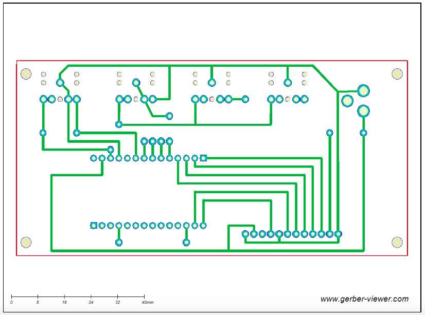
 . The major problem is you forgot to set single sided and all the traces were routed on the top layer. I also suspect that you could and probably should delete the traces connecting the top and bottom pins on the lcd to each other. I expect there is an internal connection (it would be wise to verify that before removing the traces of course