I was earlier trying to create this 3.5mm audio jack SMD by editing a preexisting part in fritzing. Here is the datasheet
. Now I am stuck on how to proceed. I am unable to create the mounting holes shown in the datasheet. Can someone help me with that. I can’t find the origin point of the hole(circle) in inkscape. Also there are two layers for the same hole in inkscape.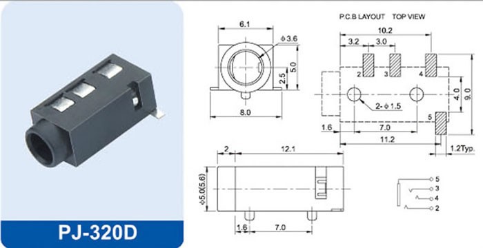
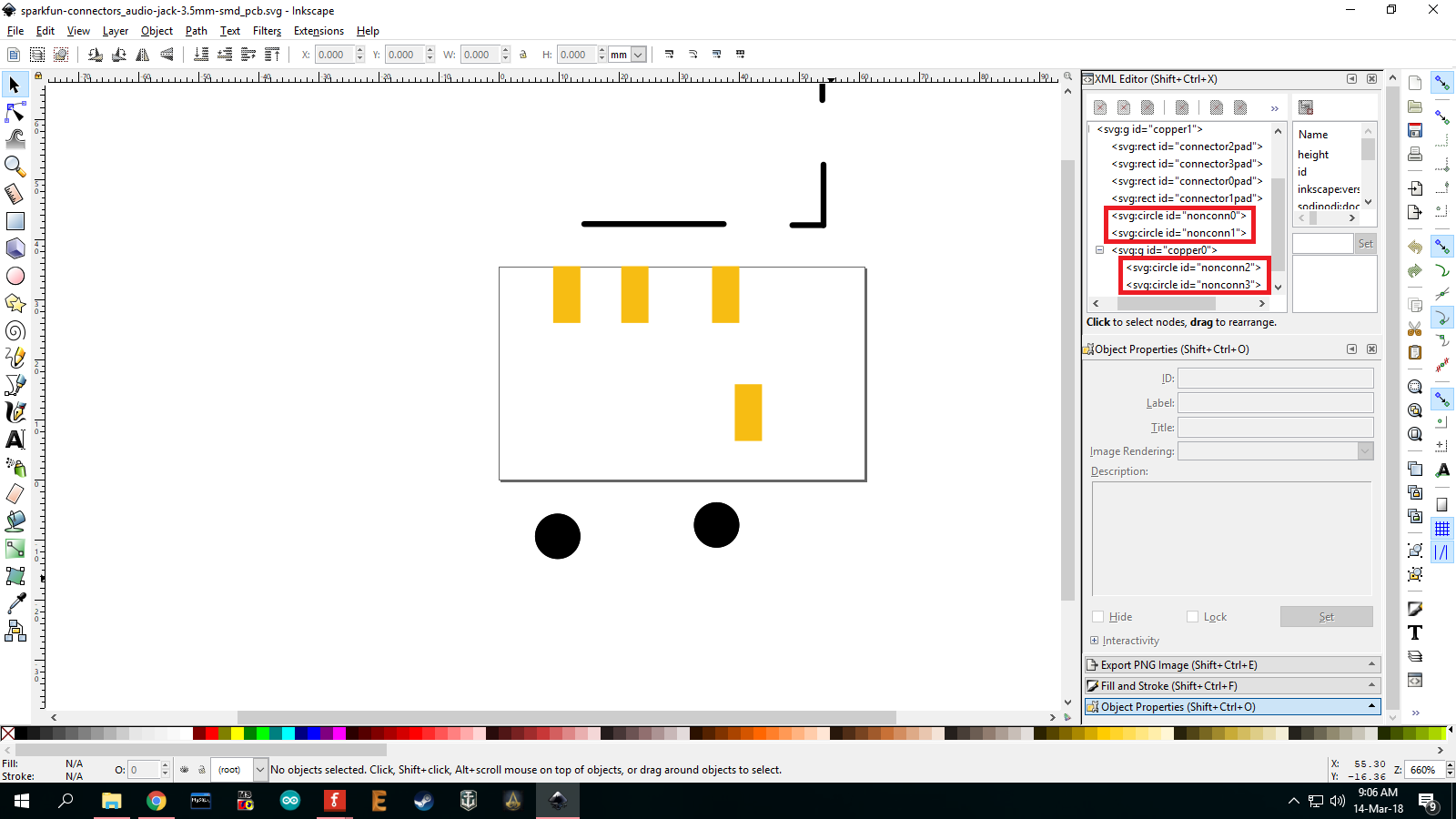
If you upload the fzpz file of your part here (upload is 7th button from the left in the reply tool bar) we can help you out. That said, its fairly easy, in Inkscape in the copper1 group create a circle with the diameter of the hole and a stroke-width of 0. That will create a hole in the board with no copper surround. You need to name the pad (change the id) to nonconn0, nonconn1 etc so Fritzing knows you want a hole there. I think this still works on smd parts but I don’t know that I have tried it. To test export the grebers and check it specifies a hole there.
Peter
I was trying to edit this part-
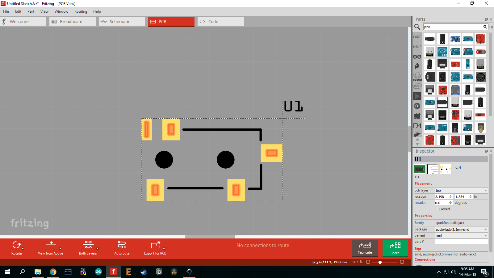
I found two layers, copper1 and copper0 in inkscape for this part.
I could not understand why there are 4 nonconn’s here. I need only two holes. I wanted to know which one to remove.
It is not letting me upload the svg file.
To upload the svg, rename it from .svg to .fzpz and upload it as an fzpz and tell us it is really an svg.The forum sometimes has trouble rendering the svgs. The best thing would be to upload the entire part as a .fzpz file though, as then we have all the files that make up the part (4 svgs and the fzp). To do that right click on the part in its bin and click export part which will write an fzpz file that you can then upload. However I can answer your question just from the xml editor lines. This is an old part, in an old format. The copper0 isn’t needed any more. If you delete nonconn2 and nonconn3 and the copper0 group that should work fine (you probably need to also remove the copper0 definitions from the fzp file as well though). From the looks of the image in the svg you may also have translates usually caused by moving elements in a group without ungrouping it (which usually removes the translates). Sometimes that causes problems in gerber generation although in this case it looks to have happened in Inkscape as well.
Edit: I grabbed the part you started from and converted it to current norms (rescaled schematic and pcb, removed copper0 from pcb). The fzp file had in fact been correctly converted so just deleting copper0 in the pcb svg should work fine for you if thats what you choose to do.
AUDIO-JACK2_converted.fzpz (5.9 KB)
Peter
Sorry I just saw your post. I followed your advise to delete copper0. Thanks to you, I managed to create the jack. Take a look. Jack.fzpz (5.7 KB)
If you want an SMD part that can be used on either side of the board you need to have copper1 inside a group called copper0 otherwise the pads will get mirrored when used on the wrong side.
Learned something new again. I was not aware of that and most of the smd parts I have seen are copper1 only. Something else to add to the parts checking script. Thanks!
Peter
It only became truly apparent in a thread about custom copper logos where I had helped make a part with copper1 only and when used on the back the words were backwards.
Your part is mostly OK, except that nonconn1 is an ellipse rather than a circle (usually caused by removing a translate, but there may be other reasons as well). If you export the pcb as gerbers (file->export->for production-> extended gerber) and look at the gerber layers with a gerber viewer (I use gerbv) you will see one hole is producing a drill hole (it is in the drill layer) and the other (which is the ellipse) is not but rather is a copper pad. To fix that, select nonconn1 in the xml editor and change rx and ry to be the same value (I copied the r value from nonconn0 to both). That will make both nonconns holes as you intend. You may also want to copy the breadboard, icon and schematic files from the Sparkfun jack part so you new part has all three views (or if you just need the footprint leave as is). With the change to nonconn1 your part looks fine.
Peter
Unless I’m missing something (which as you know is always possible  ), I think the two layer approach is only needed for parts with copper logos on both sides. This is a png from gerbv with the corrected jack part above with only copper1 defined. The one on the left was switched to the bottom of the board in inspector and the one on the right is the default top of the board setting. The pads aren’t duplicated as far as I can see. Am I missing something here? I suspect the addition of the copper0 layer is what causes the pads to be duplicated and may be fixable by removing the unwanted copper layer definition in the fzp file (although you would need to do that by editing the file I expect).
Peter
Interesting. My first guess would be since this part was created originally with both copper0 and copper1 to satisfy the need to have a copy for each side and then changed to only have copper1 it may be allowing this to happen despite not having one within the other. The copper logo thing is actually just an SMD single pin part so the rules that apply to it must apply to these as well.
My second guess is maybe it just mirrors the individual pads and since these pads are rectangles it doesn’t matter. But if the pad was non-symmetrical it would show up. I say this because the copper logo thing was in essence just a single pad that got mirrored.
Ah, yes I had misunderstood what the issue is. I was expecting the pads to be on both sides of the board. All the cases I’ve seen have had symmetrical pads, so I expect you are correct if the pad is non-symmetrical that the bottom one will be a mirror image of the top and need more adjustment if that isn’t what you want.
Peter
Yes and if you put copper1 inside copper0 then it allows it to be on both sides without the possibility of being wrong. So I think it would be best if your script did check for it just in case a part has a non-symmetrical pad.
Thanks didn’t notice that. It worked.
So for THT it’s copper0 inside copper1, and SMD copper1 inside copper0.