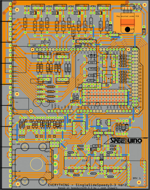
I’ve got a through-hole design which is, unfortunately, wanting to route lots of tracks on the top of the board.
Unfortunately, Fritzing wants to use component legs as vias. This means soldering on the top of the board as well as the bottom. Except because the components are flush to the board, soldering on the top is impossible.
Is there any way to persuade Fritzing to only ever connect to components on the bottom of the board? I want all routes through the board to happen at vias, because I’ll be able to reach those.
While I’m not sure I understand the question entirely a few options (probably none of them optimal): use a plated through board (i.e from one of the board fabs) so you don’t need to solder to the top (soldering on the bottom will wick up to the top via the plate through). Manually place vias on any trace that routes on the top, although you then need to ensure there is a connection on the bottom to the affected pin from the via (which may not always be possible). Fritzing supports single sided boards, but then it won’t put traces on the top layer either. Or someone else may have a trick I don’t know about.
I’m making my own board, so plating through isn’t an option. And the design is far too complex for a single-sided board — I’ve been trying, but half the traces need to go through the other half… I’m connecting 12 lines from one IC to another IC with a different pinout.
I could place manual vias but at that point I’m effectively manually laying it out myself.
It suddenly occurs to me that what I want is effectively the exact opposite of SMD. An SMD component can only be soldered on the top of the board (because it doesn’t go through the board). I want my components to only be soldered on the bottom of the board (because I have no access to the top). Fritzing understands SMD fine.
I could switch to SMD. What’s the footprint name for squashed-bug PDIP, where the pins are bent back and soldered flat on the board?
Usually something along the lines of soic number of pins. Probably easiest to find an existing IC with the correct number of pins in core and see if it has an smd version.
Just put in lots of jumpers. It’s not like you are in production and you have to cut costs by reducing their number.
You could also double load the board and place components on the bottom side.
I think the problem is they are trying to use autoroute which as most of us know does not work well. I have never used it other than to test it quickly and see it is useless.
It’s hard to tell exactly what he wants by the post.
Not even a $10K EDA can autoroute well, so it’s pretty much manual even for complex stuff. Altium has a good feature where traces get pushed automatically when you manually route - even they know autoroute isn’t great -
Latter on he goes on about squashed-bug, so maybe he is thinking of point-to-point on a level on the bottom side just above the traces. ?
Be honest why can not make the boards 2-sided? Yeah you can DIY the 1-side and it does not save anytime on the route thing. Just turn to 2-side. You can find many companies offering good price prototyping service for 2-side pcb.
I want to make a double sided board. But I can’t solder through-hole components on the side of the board where the component is, because the component’s in the way. The solder pad is inaccessible. I can only solder them on the other side of the board where the pin is sticking out. This means that I can’t connect component-side tracks to the component leg.
I asked about squashed-bug ICs because that would let me surface-mount my DIP chips; because they’re surface mounted they can’t be vias, so don’t cause the problem. However there don’t seem to be any suitable footprints, so.
It’s not quite as simple as editing a component to remove the component-side connection, either, because I need to make sure that fritzing knows not to put tracks where the pin is…
He likely did a reply (as I usually do) on the bottom of the screen rather than a reply to your specific post (as I remembered to do this time ). The general reply doesn’t send you a notification, only a reply to your post or a mention of your id does.
Are you aware that commercial double sided boards have plated through holes? That means if you solder the bottom of the pad, the solder will flow up the plating and solder the top as well so it shouldn’t matter that you can’t solder the top side (as long as the component won’t short the pads with something conductive). The plating in the hole connects the top to the bottom electrically as well so even it the solder doesn’t flow there will still be an electrical connection. If you do need an odd smd footprint if you can provide a reference it is easy enough (at least for me, with experience making parts) to create one. We only need a specification to follow.
Yeah, but that requires me to use professional board manufacturers, which I don’t want to do — its not just the price, and they’re not cheap, it’s the multi-week turnaround. I can make a board myself in an hour (but I can’t plate them).
Then yes, you are correct plating through isn’t available at home. Then the other offer stands, if you supply a smd foot print you need I can either point you at one or make one (they are fairly easy given a spec and experience making parts).