When I design things on the breadboard and switch over to pcb view, the connections arent all in the right place:
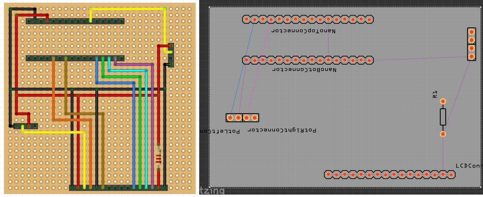
Why does that happen?
When I design things on the breadboard and switch over to pcb view, the connections arent all in the right place:
Why does that happen?
The views are independent in layout. You need to move the parts in pcb view in to the same positions as on breadboard if that is where you want them (I assume you have started to do so as by default they will be mostly on top of each other in pcb view). The connections via the rats nest lines will match between views unless you make changes in multiple views at which point it is possible to confuse the data base and get a corrupted image. It is possible to recover from that by deleting all wires in all views and doing all the wiring in a single view and then following the rats nest lines in the other two views.
Peter
Are you sure this is the cause. This is the main reason I use Fritzing over Eagle. I like that I can work mostly in PCB to create the circuit then go to Schematic and make sure I got things correct and if not fix it and go back to PCB and re-route those traces. Through out my use I have never had a corrupted database. Could this be because I never use Bread board or maybe because I am Linux?
The usual case I’ve seen is a part reversed between breadboard and schematic or pcb (i.e pin 1 pin 2 in bb but pin2 pin1 in schematic) with manual connections made in both breadboard and schematic (or pcb). The backwards connection causes routing issues and bogus rats nest lines. We used to think the only solution was scrap the sketch and start again, but I found if I removed all the wires from all three views (including moving things off the breadboard if it was in use) the database would recover. That isn’t much easier than starting again though. If you don’t mix up your connections between views I think things will work fine. For newcomers make all your connections in one view and then follow the rats nest lines works best.
Peter
The only time I see FZ wrong is when the person makes a mistake.
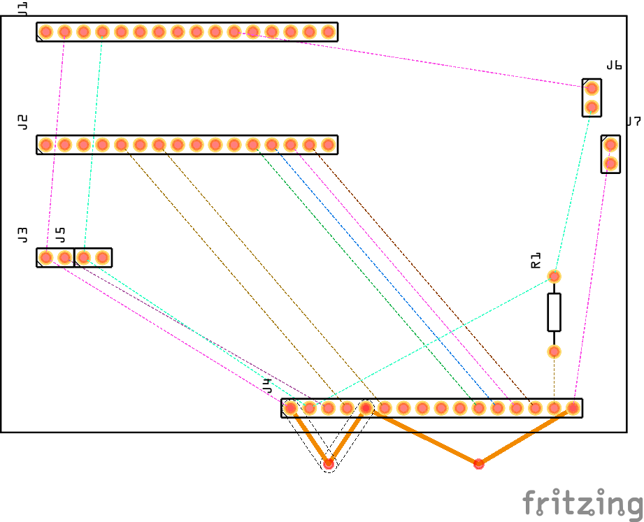
I bet you havn’t paid attention to the JP# numbers so that are in the wrong positions in PCB view - right-click show label -.
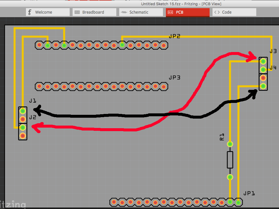
You can’t join wires with links between wire bendpoints in BB view - it’s a legacy of the breadboard -, you have to run a wire to a hole from all ends for it to be connected. To check you click on a pin on the header and if it’s connected all the connections will turn yellow - it is not fool proof in all instances -.
See that black wire from the 2 pin header on the right to the 16 pin at the bottom, it is a continuous unbroken wire between the pins with that horiz black wire sitting on it’s mid point connected to the hole but not connected to the other wire.
EDIT
Sorry if you were trying to read this in the 100 edits I did because I was learning how to use pref broad myself.
Hi Old_Grey,
I did see the JP#, I actually named them so that I could keep track of them.
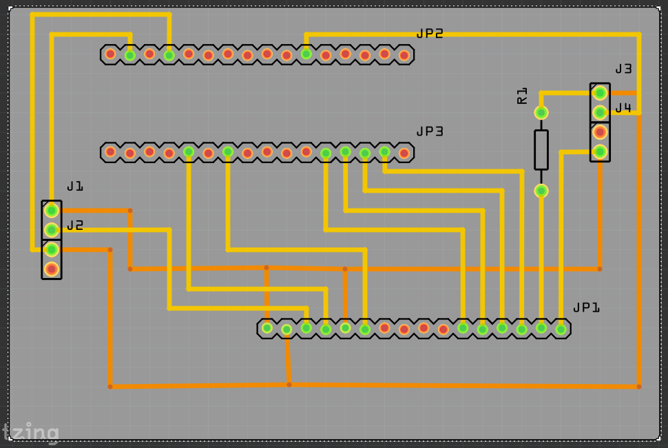
But as you can see, the LCD header at the bottom has no lines connecting to it except for the R1 in PCB view, whereas in bb view its got a bunch of connections. If I click once over each header I can see the yellow dots blinking where it has bendpoints and connections to the other headers.
If you upload you fzz file from the sketch we may be able to point out what is wrong (and we may not, if the problem was an incorrect route earlier that has now been removed, as that leaves the database corrupted even after the offending line ir removed). To up load use the 7th icon on the left on the reply bar (which I expect you already know) and select the fzz file.
Peter
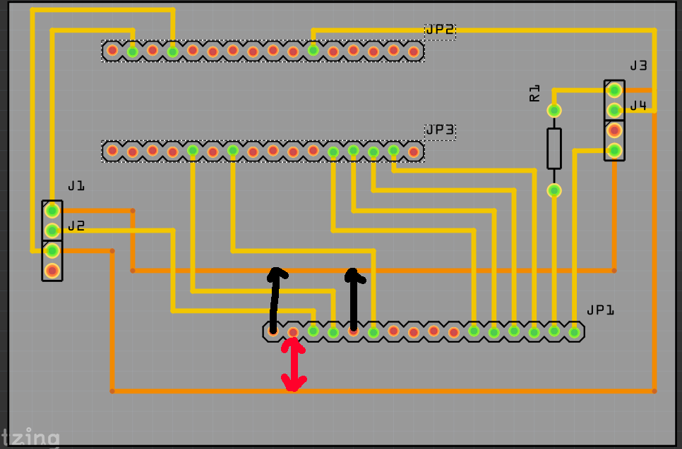
I’d say (from the pattern of error, (all the connectors shorted to each other on the connectors) the cause of this was likely at some point the perfboard was strip board (which will short all the connectors together) and once that route is in the database its difficult to get it out again. One solution is to, in breadboard, delete minus (note the minus, which leaves connections intact and removes the part, delete will remove the wires) the perfboad. That (at least after you move the connectors to refresh the rats nest lines in the other two views) clears the shorts from the database and you can then re add the perfboard in and it will work correctly. It looks like you will need to delete and rerun all the wires (one at a time to preserve the current routing use delete and to remove them all and start again) to get the rats nest re established unless someone else knows a trick to get the connections to refresh (moving the connectors does some of them).
Peter
I can see somethings not connected.
EDIT
Your right it’s corrupted. You have to start again with a new one and only work in 1 view, like my one above.
I think the SCH is like the Alpha, because Delete Minus in BB doesn’t remove all the ratsnests in other views. I would say start again with the knowledge of how to do connection effectively, and to keep in 1 view only and the do the others after and trust FZ’s ratsnests.
Here is mine Coffee.fzz (11.3 KB)
Ok so I started a new file, i immediately deleted the breadboard that gets added by default and moved over to pcb view. I added a perf board and the header pins and resistor. I then started to make connections and ran into an issue that I didnt have in breadboard view, which is, how do I make the black wire ground connection on my original post which goes all the way from the left side of the perf board on a header pin, over to the right side, through some wire-wire connections and then over to the other header pin? The same for the Vcc red wiring.
This is what I have so far but it wont let me drag a cable from the a hole that already has a wire connected to it.
Assuming a double sided board you need to change layers and route the ground wire on the top layer or insert a via between layers to continue the wire on the other layer. If you are going for a single sided board you would need a a jumper wire (there is one available in the pcb section or the core parts bin) or creative routing to avoid the conflict.
Peter
Ok Ive got it down to this.
I moved both Gnd & Vcc to the bottom layer.
I placed the lcd-data wires from JP1 to JP3 on the top layer.
Now I need to make 2 more connections from JP1 to GND and 1 more connection from JP1 to Vcc. I was thinking of interconnecting to the runs of GND & Vcc on the bottom layer as they travel from left to right but I dont know how to do that.
Actually there are 2 issues, one is the routing and the other is the actual connecting.
As for routing, I would need to route both of them on the bottom layer, but that means they would cross. So I guess a jumper is inevitable.
As for the actual connecting, how do I make a connection to the middle of another wire?
It looks like J1 is Ground and J2 is Vcc so a wire on bottom layer to the appropriate pin on jp2 does ground and a wire on the top (which may cross the ground wire on the bottom) on the top layer will do it if they need to cross. Looking at your original breadboard I’d run the two power runs on top layer J1 to pin2 of Jp1 and J2 to pin1 of Jp2 from below jp2. That leaves you room for the other 2 wires to the nano on either the top or bottom of the board as you choose.
Edit: looks like an edit occurred. With the current drawing, on bottom layer connect pin 1 of jp1 to pin 1 of j1 and then just drag the resulting wire down to connect with (and overlap) the wire it wants to be on the bottom. For the other one top layer across to pin 1 of J2 no jumpers required (you can usually avoid jumpers by creative routing on two layer boards).
Peter
Ok I moved the gnd run anove JP1, so I wont have to cross wires. The problem now is the actual connecting. When I drag a connection from the JP1 pins to the wire runs, no connection is made. Do I need another component?
A lot of routing is puzzle solving. Here I ran loops so I didn’t need jumpers.
https://scontent.fsyd3-1.fna.fbcdn.net/v/t31.0-8/19390605_10211177024435237_5358132903310226007_o.jpg?oh=52f53b897bf54ce9be4cc1c8a9245aad&oe=5A35321A
To join mid wire put a bendpoint on it, and run from pin to bendpoint. Or hold ALT down and click on bendpoint, and run from bendpoint out.
Also note no 90º bends. It’s good practice to use 45º.
EDIT
There is also a thing called a plated via in CORE bin that connects both layers through the PCB. You run a trace to a via from one side. Then run from the via to another via on the other side. And then run that via to the part back on the original side. It saves doing a wire jumper.
Thanks,
I got it like this and here is the fzz. Does this look right?
CoffeeHumidityMeterv2.fzz (8.5 KB)Looks fine. Two things you want to do before ordering a board though, run design rules check (I don’t expect it will have issues, but always best to check) from Routing->design rules check in pcb view. Then export the layout to gerbers via file-> export->for production->extended gerber. Check the resulting gerber files with a gerber viewer (I use gerbv from the geda project) to make sure the gerber output matches the image above. The gerbers are what the board house will actually make the board from and if they aren’t right, neither will the board be (and sometimes Fritzing makes mistakes in converting to gerbers).
Peter
Ok I got:
“Your sketch is ready for production: there are no connectors or traces that overlap or are too close together.”
I moved over to another project and I did get some rule violations so Ill post in a new thread. Thanks!
Some tracks look wonky. When you add a bendpoint to a wire you have to grab it and re-snap it to the grid. Grabbing a junction is also a good way to know if all the tracks are connected.

