I’m designing a custom pcb board with Inkscape and things are going fine but I wanted to add a cutout to the pcb. I’m going to use OSH Park and their guidelines say that the “Board Outline” layer needs the text “cutout” in the cutout for the fab. Has anyone done cutouts with the pcb board with Fritzing and used OSH Park? If so can you share some notes here?
A couple of days ago, I was researching exactly what you are trying to accomplish now (figuring out what works and don’t work)… and using OSH Park guidelines. Post your board.svg… Although, for some reason SVGs will not post on this forum and no one can solve the problem… So you may need to use http://www.imgh.us/index.php or something else… and I will fix your file with the guidelines from what I understand. then you can open it up in InkScape to see what the file is suppose to look like. Then when it comes back for the fab house you can tell me if it works and send me a pix.
I believe I am going to have to write an article on this subject just because it is not very well document…
Ok cool, that svg upload thing is annoying but anyway here is a link to the file I’m using http://imgh.us/d10.svg
Everything on OSH Park looks good except the cutout holes in this version. I didn’t put the “cutout” text in board outline either but when I did the text did not show up. Also you will see that OSH Park’s uploads didn’t render the cutouts right in the board top, bottom but that might just be OSH Park. I will ask them soon if this is expected.
OSH Park board top:
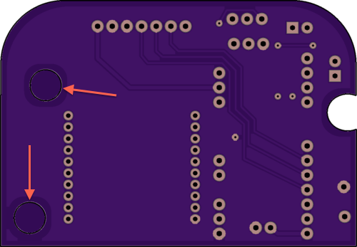
OSH Park board bottom:
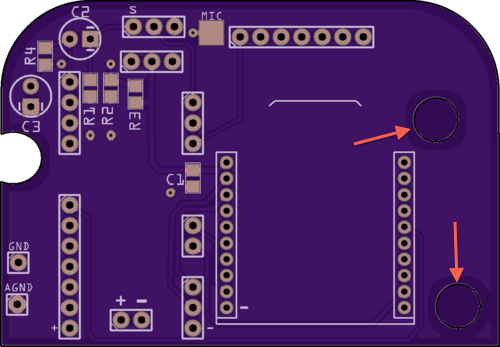
OSH Park board outline:
Hi Duff,
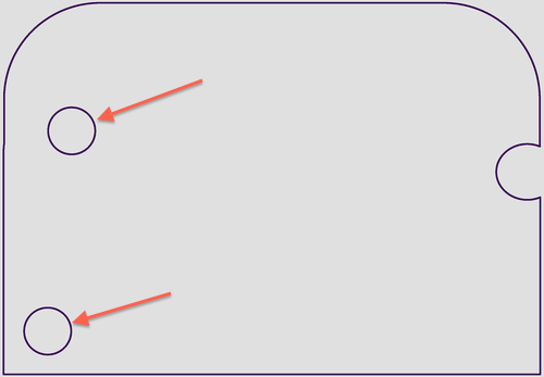
I think you are all right, the internal cut outs don’t show up on “any” of the gerber test programs. Don’t know why that is… But they all show an outline where the cutout is to be placed on the board layer. OSH Park says to write CUT OUT on the dimension layer, but is not necessary… Fritzing does not have a dimension layer. I tried everything possible to write it on the board layer… weird things happen. The only thing I would do is to add CUT OUT inside the two little circles on the silkscreen layer on both sides. I normally add it to silkscreen and silkscreen0 on the board shape.svg.
I don’t remember, but I think there is a place for add instruction when placing your order from OSH Park. Please let me know how this turns out and what OSH Park tells you to do.
If you go the OSH Park shared projects and type in Pi Hat, there are a couple of Hats that have cutouts with CUT OUT written in them.
I noticed that any node in a copper group in a part becomes a hole, can you add copper group to a board.
The hole it to big for a drill… it need to be a cutout.
You can put circles in copper so I assume you can do rectangles also, and anything in copper seams to be cut out.
Please clarify… I don’t quite understand you question…
When you stated “copper group to a board”, are you referring to the board-shape.svg?
I was wondering if you can add a copper group to a PCB svg, because anything in copper gets drilled.
Nope… the PCB.svg only has three layers: board, silkscreen0 and silkscreen, no copper or drill layers. The board layer can only have one “boardoutline” object, (this can be a combined object), other objects in the board layer are place markers for holes, connectors, pins, etc. and do not get transferred to the gerber… unless you forgot to label the boardoutline object, then everything goes to the gerber and wired thing happen.
Silkscreen is the front of the board and silkscreen0 is the back and normally are just the outlines of the board and cutouts. These are on the silkscreen layers so you can put anything on them that you want to be printed on your board along with the rest of the silkscreen.
I suppose if the holes don’t get cut out… you can always get the ole Dremel tool out and follow the cutout silkscreen lines… 
Worse case you just grab a hole from the bin and put it over the hole cutouts.
I don’t know anything about making a PCB but I had a play around and that drawing is not a path, even though it say it is, so you can’t subtract/difference holes, so you can’t add cutouts.
I made 2 rectangles, converted them to paths, difference one from the other, add silkscreens to XML, export as gerber, and there seams to be a cutout in GerbView.
Will have play latter.
How big a hole does it have to be, to be a cutout and not a drill… If a hole is to big to be drilled, does it automatically go to the router program to be cut out… Does the mounting holes in a board like R-Pi get drilled, routed, or laser cut? With today’s technology, what gets cut/drilled with what? (routers, drills, and lasers). Maybe I need to contact OSH Park and see what they say… 
I haven’t looked into this much since i just moved but will try to get an order into OSH Park in two weeks. I’m also looking for other examples on their website of cutouts to see how they look.
Ok, I got the ok from the OSH Park guys today and it looks like the way I did those cutouts are fine. He said as long as it shows up in the boardoutline the fab will do the cuts. He didn’t mention anything about placing text in that layer either. I will send this board out soon and follow up here on what happens.
duff,
My appreciate your “how to” on using Inkscape to create custom PCB… would you be willing (PLEASE  ) to create a "how to’ on using Inkscape to create the circuit SVG (used in schematic) for parts?
Probably not critical for PCB outlines, but I would change the grid to 0.254 or 0.100", which is the conventional spacing. I’m finding too many parts, even in CORE, with less than perfect pin alignments.
Dang! Must of taken you every bit of five minutes to write this up… just kidding… Nice job! I know CorelDraw like the back of my hand but even I can use this to learn more about InkScape…![]()
I wanted to make it with less slides but I know from personal experience that those little steps in-between make the difference of getting it to work or being very frustrated. If anything is unclear or not intuitive let me know. Plus I hope I got all the steps to get it the first time!
I have been wanting to make custom pcb’s for Fritzing for a year or so but every time I tried it just didn’t work so I would give up. I had some time to figure it out and I thought making this would help someone in the future. I’m novice with Inkscape but for basic things like this it is actually not that bad once I committed to doing this.
Maybe we should try to persuade the admins to make a wiki for tutorials so they can be in one place? I’m planning on expanding this to cutouts also, since that would be the next logical step.