I just recently ordered my first PCB board and I didn’t realize that the holes for the Barrel Jack are slated for a barrel jack pins that would fit in a breadboard. The pins of the barrel jack I purchased are more of a flat pin, which I assume is designed for a PCB board? The holes on the PCB are tiny and I’m just so new to this I don’t know if I made a mistake or manufacturer did (I’m assuming I did).
The Linear Voltage regulator (7805 TO-220) fits in the PCB board, but it’s kind of the same. I would like it to sit flush on the board (not a big deal), but the pins flatten out and get larger towards the base if that makes sense.
Everything else seems to be good (for my very first design) if someone could help me find the correct part or make the holes for the Barrel Jack bigger I would greatly appreciate it! Please keep in mind I am very new to this side of things (I’m a software engineering student, with one class on the embedded side).
Another quick question, on the final design of the PCB the bottom of it does not have any of the traces that were supposed to be on the bottom, I’m assuming this is ok/supposed to be the case?
Looks like you copper filled after you placed the parts, but then put traces on the PCB so they are on top of copper. Click on copper fill on the PCB, delete, and then copper FILL if you want to keep GND traces separate, or copper GND if you want GND to be all in 1 plane. You must GND seed pins for GND fill.
Slots are a problem that I’m not sure about in FZ, because when you look at the drill.txt file they are always round.
To be clear, the Ground copper fill needs to be the very last thing I do? So, I should delete the GND Copper fill, get everything where I want it and then add the Copper GND? All of the traces I have on the bottom are GND, except for one partial trace that goes to the bottom with vias. Also, does it make a difference that I cannot see the traces on the bottom of the PCB, or is this not going to work correctly? Also, when I add the Ground Fill, I add it to the bottom layer, this is the correct way, right?
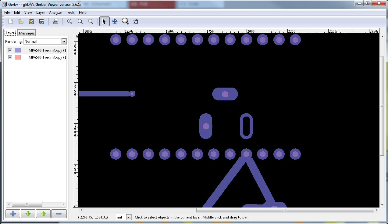
I found one barrel jack in the parts that seems to have oval “slots”, is this ok you think? I added it in the design below. How do people add parts with slots to a PCB usually?
Yeah GND fill last. You can also adjust the keepout if you want more gap.
Yeah you don’t need the GND traces if you’re going to GND fill. I think people just leave them as dotted-line ratsnets. Maybe delete them, but check you have a GND seed(star shape) on all the GNDs after you GND fill. You can click on a GND pin and everything connected turns yellow.
Not sure about the jack, because the pads are oval but the holes might just be circles. I have see people use huge holes instead, but maybe put export the gerber and look at it in a gerber viewer to see what they actually look like.
It looks like you used an Adafruit part for the barrel jack, so your best bet may be to order that exact barrel jack from adafuit (I didn’t think to look at the jack part when I looked over the board.) I’d expect this jack will fit the holes in the part (as it is the product the part is for):
There is a variant in core parts from Sparkfun that has slots but note the warnings that it is experimental and the one with holes is the proven part. If you want to try the slot version, you should check with your board house if the gerber suits them. I remember a forum post where someone was trying to get slots and I think the conclusion was the Fritzing can’t easily do it.
Yes most of the Voltage regulators have pins that get larger near the case so there is space between the part and the board when automatically assembled by machine. There is a post from Old_Grey here with a laying flat version. I think this part originally had a translate in copper0 (that I figured out much later), and I don’t know if it ever got fixed. If you want to use this part, post and I’ll have a look over it to make sure it is correct.
While it didn’t come out as intended, I think it should probably work fine. All the isolated logic ground has been subsumed in to the ground fill, but even if not as intended, it looks like it should still work. The one non ground trace on the bottom looks to have been isolated correctly so it should work fine.
Sorry to be a pain, just wanna make sure I understand. So I added a GND Fill to the bottom so that is the reason I can’t see the traces I added, right?
Is this the proper way to do things or should I not add a Ground Fill and leave the traces on the bottom? I wasn’t sure if I added the Ground Fill on the bottom if that trace that goes to the bottom that is NOT a GND trace through the vias would be negatively effected?
Yeah, I checked the Gerber on the Fab site. Do you know how to manually adjust the hole sizes? Is this a Fritzing thing, meaning if I used a different PCB design tool would I be able to add the parts with slots?
Hey Peter! Yeah I cannot believe I didn’t check the part first. I saw a YouTube video that suggested printing the design out and make sure all the holes line up for parts. Is there a way to increase the hole size manually or if I used a different PCB design tool I could add slots and/or any idea if I can just talk to the manufacturer and have them put slots there
The crazy part is I do have that part! The holes for the barrel jack are the smallest of all the drill holes on the board, so I was seriously surprised that one didn’t fit.
Awesome! This is perfect, thank you!
Is this the proper way to do things or should I not add a Ground Fill or a Copper fill and leave the GND traces on the bottom and just the GND seeds? I wasn’t sure if I added the Ground Fill on the bottom if that trace that goes to the bottom that is NOT a GND trace through the vias would be negatively effected
I found this barrel jack which looks as if the holes are large enough for slots pins. Do you think this would work, I’d just need a little extra solder?
The part states this, which I don’t really understand, particularly the part about the “mill layer”…
“The slot footprint only works if the mill layer is transmitted to the PCB fab house so be warned.”
You can just grab a via and put it on the jack pad, but use a hole dia the width of the blade - this is in sketch also -.
If you already made the PCB, and there isn’t too many, I would get a rat’s-tail file and slot them myself. Then just fit the jack and bend the tabs over and solder. Conversely you could cut the spade lugs narrower until they fit. You can also drill the reg holes bigger, it’s just that you have to solder top and bottom because the plated hole gets cut in the drilling of a 2 sided PCB.
So I would just add a via to all three of the jack pads like you did here?
I see! Did you add the Ground fill to the top or bottom? Do you think this is preferable or not adding the Ground Fill and leaving the traces on the bottom? Peter spent a lot of time helping me get those bottom traces correct!
Totally no need for tracks with GND fill, you can even see in the gerbers they are connected.
I’m no expert, and all I’ve see is what this guy does, but he just leaves rats. He also leaves off the GND fill for clarity, so you have to add it before ordering. schematic v0.3.6.fzz (283.8 KB)
To my surprise the adafruit part appears to be wrong. It is set for a 0.030 in hole (0.035 is standard for IC leads, so it is small). I thought you may have an old version as they current one was updated in 2017, but it too has a 0.030 hole and their data sheet for the part calls for at least a 0.042 hole to fit the pin (they actually want a 1 by 1.6mm rectangle which would be a 0.062 by 0.039 which should likely be replaced with a 0.042 hole as the widest part appears to be 1mm (0.039in, a little tight in the standard 0.038 hole for a .1 pin). I can correct the part for you to have a 0.042 hole, if you want to rescue the current board, just drilling the pins out with a 0.042 drill should do the job. That will kill the plating through so you would need to solder both sides (which you can’t do with the ground and you would need to check if you can for the 12V pin whihc is on the top, if the part is on the way so you can’t solder it this won’t work. Another board package such as Kicad or Eagle may be able to do cutouts, I think it depends as much on the board house being able to do that, and it is likely extra cost (as they need to set up the tooling to do it I expect). I don’t really know because I don’t often make boards.
A ground fill for the high current path is a good bet. Remembering that I don’t do boards much, I would be tempted to ground fill the motor ground and leave the logic ground traces out of the ground fill so that they are isolated from the motor ground. That said, with a ground fill covering the whole board you have a very solid ground available and the isolated ground is less necessary.
Noting I’m on shaky ground here I expect this is a layer in the gerber output. I just tried the slt version, and Fritzing doesn’t generate a mill layer in the gerbers so I expect it won’t work from Fritzing. That matches what I remember from a similar discussion a couple of years ago.
I just had a look at the part and it looks fine, no translates in the copper layers. I see there is a comment that it was fixed so it is probably the part where I found that translates in the copper layers are a bad idea (the check script will toss an error on them these days).
If you can find a 0.042in drill and drill the holes in the current board out to 0.042 and the part fits I can change the adafruit part and offer it back to them as a correction for their part so someone else doesn’t get caught if you like. From the data sheet the 0.042 hole should fit the pin reasonably well.
Just make sure you adjust the inside diameter of the via for the width of the lug, because I just fudged that 2mm via.
Remember don’t get anything made until you print the gerb and see if stuff fits, because we don’t know how good the position of the holes are in that part.
So, I’m not really sure what you mean by the “width of the lug”, what is the lug? I’d change this in the spot on the via that says “Ring Thickness”, right?
If I keep the board the same with the traces how you helped me fix in the other post, you think it would be best to bring the Logic Ground traces to the top of the board? Then I would leave the Motor Ground traces on the bottom of the board?
To be honest, I would rather call it a learning experience and order new ones. Are you saying you can fix the Adafruit Fritz part? If you’re able to fix the part and wouldn’t mind, that would be awesome!
Edit: Oh are you saying to drill a hole and see if it fits first before you start messing with the fritz part? I can certainly do that! I’ll try and find a drill bit that size tomorrow.
What old_grey said about adding a via to the jack pads seemed like and easy way to increase the hole size?