INK (GLCD) Display Part (NOKIA-5110)

These are useful, low-cost, low-thickness INK display’s with a Backlight.

I made three Variants of the connections:
• Variant 1 - Top Row
• Variant 2 - Bottom Row
• Variant 3 - Both Top & Bottom Rows with internal connections. Pads will be placed on the PCB - if you don’t want the pads for an un-needed row, use a different variant. Variant3 helps routing traces as needed without needing jumpers if they needed to crossover a trace.

Much thanks to ‘vanepp Leader’ for insight on Part Making.

[UPDATE - REMOVED the Files with errors]

1 Like

Over all a nice job (I have a previous part from someone but I like yours better :slight_smile: ). These are a nice cheap display and there is a nice library available from Sparkfun. That said your part has a few issues (mostly in schematic, and mostly style, yours works just fine mostly). Both breadboard and schematic are lacking the correct layerIds. The only thing I know that affects is svg export of the part from Fritzing will fail. The holes in pcb should be labeled nonconn0-4, with a stroke-width of 0. This is secret Fritzing code that causes the gerber output to only put the hole in the drill file (yours will work but it puts copper on the copper layers which the drill will then drill out). I changed schematic to look like this (mine on the left yours on the right):

nokia_schem

The wire on yours connects to the middle of the pin (rather than the end as is desirable) because you don’t have a terminalId defined in the schematic svg. Without the terminalId the wire connects to the center of the .1 in long pin which isn’t what we want in this case. Below is a modified (with a new moduleId so you can load both parts at once) copy of your Nokia 5110_INK_Display_BtmRow.fzpz part with my changes (in addition I rescaled them all to the standard scale as well as fixed the layerIds).

Nokia 5110 INK Display_BtmRow.fzpz (7.3 KB)

Peter

1 Like

Peter, Thanks for the comments…

Regarding the re-name of Holes to “nonconn”. Agree and started to do it (as shown on PCB in screenshot).

Regarding the Schematic - graphic: Was torn between similar to yours and what I ended up with. Preferred mine for economy of size. Also, as mentioned in my write-up in post; the fonts are not as Fritzing wants (my eyes are 70yrs old and cannot see the light gray tiny fonts).
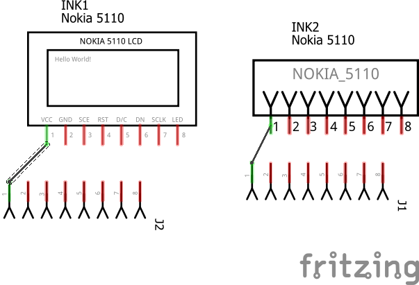
[Also, not mentioned - For the Two-Row Version,I chose to sequentially number the pins rather than duplicate them as that’s how I wired my hardware.]

Regarding the Wire connects on the terminals. Agree (though I left them as-is because it seems many/most of the parts I use also connect at the center. But, at the end of the terminal makes much more sense and will change them).

Scaling? Why did you rescale them and what was wrong with the scale? My Inkscape is set to Inches and the default of 96px/inch.

Really, really weird! Re-Opening the files in Inkscape:

Hole stroke-width: they were set to 0 but, reopening the files shows them at 0.01

Lacking correct ID’s… even more weird - you can see in the image that all ID’s and Layer names are set to what I believe is correct. So, I’m, either not sure of what you’re referring to or, something software-wise is happening???

You mention an SVG issue if exporting from Fritzing will ‘Fail’: The files I posted were Exported from Fritzing so, if you were able to open them, and, indeed check-out the part, well, I’m further puzzled…

I see your files are nicely flowed and you must have manually re-arranged/re-flowed them - did you do it in an editor? Perhaps your editor removed the ID’s ( I’ve noticed that Inkscape sometimes does a re-naming if it doesn’t like an ID or is duplicated or it’s contents have changed. FYI - I use a Mac.

[Rather than updating my last post, I’m doing via a Reply]

I updated/changed my files to reflect:
• All file’s:
Changed Hole Stroke-Width=0

• Schematic’s
• Terminal End connections
• Changed graphic to Box with single-lines (not Y )
• Changed sequential numbering to Duplicated 0-8

• PCB’s
• Holes: changed ID to ‘noconn’

As said/shown in previous post, all files have correct layer names and ID’s. I opened them in several different editors (xCode, BBedit, eclipseNeon, OpenOffice, TextEditor) all show ID’s correctly.

Exported them from Fritzing.

I think the only remaining thing for me to understand/change are the ‘Scaling’ you referred to… However, given that, in Inkscape, 96px = 1inch, logic suggest scaling them by 1.0427. Rather than rescaling for these re-posted parts for you review, I’ll wait for clarification of ‘scale’…
And, any ID’s that you mentioned where I may be missing a point you’re making (sorry, old and slow).

Thanks again

As always, your part your choice :slight_smile: I prefer my version and prefer (in case of later mods) to have the text as text elements so later changes are easier but your method certainly works as well (it is just more complex if you want to make changes later as you have to delete the path and redo the text).

The parts format document calls for the viewbox to be set to 1px = 1 thou inch (which at 96dpi in Inkscape is a scale of 10.41667 in the document properties page. That also makes setting the hole size in the xml easier so I generally do it. It won’t affect operation as long as the height/width are set in either inches or mm so Fritzing knows the real size of the document. If the default px (and no units defaults to px) is used Fritzing will make a guess as to what the dpi was (72 for old illustrator, 90 or 96 for older/current versions of Inkscape) and sometimes gets it wrong and causes scaling issues in parts.

What can I say? :slight_smile: Inkscape does odd things sometimes (but I’m far from an expert on svg editing so there may be a good reason for it). I think it converts to some high resolution internal number representation and sometimes has round off effects. That said when I reopen the pcb svg on Windows in Inkscape the stroke-width value is still 0 as I expect.

The breadboard svg is actually a copy of the pcb (as is icon). Schematic is really schematic but is partially wrong in that there should be only one group for the entire document and it should have the label schematic not silkscreen (which is only used in pcb) or what ever is in the fzp file (which will usually be “schematic”) in the layerId line. From your Btm_row part above the fzp file has:

  <schematicView>
   <layers image="schematic/Nokia_5110_btm_3f8387282d7ce92c6d9b0502a0db1f25_1_schematic.svg">
    <layer layerId="schematic"/>
   </layers>
  </schematicView>

meaning the group currently set as “silkscreen” should be “schematic” (which is somewhat below it as another group). Same with breadboard and icon, there should be a single group for the whole drawing with the id “breadboard” (which is set in the fzp file as well). Icon is typically a copy of the breadboard svg, and Fritzing doesn’t seem to care that it isn’t called “icon” as specified in the fzp file. I suspect (but haven’t tried) that the text in group silkscreen will be omitted from the part during an svg export.

I wasn’t quite clear enough, the part exports and works in Fritzing just fine with incorrect layerIds. However if you put the part in a sketch and then do a file->export->as image->svg of one of the views when a part has has an incorrect layerId, that part won’t be in the resulting svg but the other parts (with a correct layerId) will. It is fairly minor but annoying because it causes questions when someone uses such a part in a sketch and then asks why the part doesn’t show up on svg export.

The formatting is a result of two things: I ungrouped all the svgs (which removes transforms and unneeded groups that the Fritzing exported likes to add and then ran it through my parts checking python script which converts silkscreen color to black (to show up in Inkscape), converts style commands to inline xml (because sometimes Fritzing won’t deal correctly with style commands in all cases and inline is equivelent) and removes the trailing px from font-size statements which Inkscape puts in because CSS requires it, but which breaks Fritzing (as it converts font-size with a trailing px in to a 0 font-size but only on export). As part of checking the part the input formatting is lost so the script finally runs the xml through a pretty printer which is what gives the clean output (until Fritzing’s exporter adds the groups again.) Hope this helps! Parts making is complex and poorly documented, so we tend to learn as we go.

Peter

Just saw your post after I posted…

Yeah, clearer documentation would be helpful and would eliminate back-and-forth exchanges. Thanks for hanging with me on this!

Yes, in first group of parts I did use the ‘Reuse’ feature for some items - guess that’s not a good idea. The files I just posted do not reuse files.

I’ll review your recent post and update as needed (however, it’s unlikely I’ll change the font size BUT, I will change the text Path’s to Text (paths also make a hassle to edit the text…).

Thanks!

Happy to help, lots of folks helped me when I started a couple of years ago. In theory (but I’m not sure about practice) Fritzing will only take ocra and droid sans fonts and anything else needs to be converted to a path. That said I think I have seen examples of text in other fonts that Fritzing rendered. I’d suggest trying a test case before doing a large conversion to make sure Fritzing will accept and render another font.

Peter

I opened your file in BBedit so I could more clearly see what’s going on. Real simple!!!
It turns out that the Fritzing documentation I read regarding building a part is so bad and correlates very little with what you did.

Before starting out, I reviewed the doc’s and did outlines of ICON,PCB,Schematic and BreadBoard files per the doc’s. Wasted a lot of time - guess the learning was worth it but, not a good representation of Fritzing…

The doc’s call for different organization structure which led me to most of the problems. But, now, with your help and clarity from your file, I see the light… and it really is simple.

FYI - Two of your files changed the pads from Circles to Ellipse’s. That happens in Inkscape if just breathing on a Circle.

The doc’s call for sub-level grouping of connectors if they’re part of a buss (as in the TwoRow version). That’s how I did that version. But, now that I see how different your file structure’s are, I wonder if the Buss is even necessary since the editor panels have an Interconnect feature… ?

I’ve used both OCRA and Droid-Sans for part&pcb and that font is good for me (just can’t use a tiny size or light grey)…

I understand the scaling requirement.

That is likely an artifact of the rescaling (possibly due to rounding). After a rescale circles are often an ellipse with an rx and ry rather than an r. My script looks for that in the pcb svg (but not the others) and flags it as an error because the gerber output won’t create a hole for an ellipse. In breadboard or schematic it usually isn’t an issue.

I’ve not seen that documentation, it may be for an older version (much of the documentation around is). All I’ve ever used for buses is a bus definition in the fzp file which defines the bus name and specifies which connectors are in this particular bus. The check script checks to make sure the connectors exist in the svg, but I’ve never had to put them in a special group (and the current parts file format document doesn’t specify any groups needed) and usually leave them in the layerId group. The new parts editor internal connection feature creates the necessary buss definitions in the fzp file. If (as in this case) the pins are connected together internally to the board, then they should be bussed in the fzp (or via parts editor) so the nets come out correctly.

Peter

It’s possible I’m misunderstanding the image below (from https://github.com/fritzing/fritzing-app/wiki/2.1-Part-file-format )

54 PM

If you are thinking that the “bus0” and “bus1” ids need to exist as groups in the svg, then yes you have misunderstood. They only need to exist (and be unique) in the fzp file and connector0, connector1, connector2 and connector3 need to exist in the fzp file and contain a pin svgId definition such as svgId=“connector0pin” that exists in all the svgs and everything is happy. The bus definition stuff is only in the fzp file.

Peter

Yes, it is for the fzp metafile… It’s all clear now.
Thanks