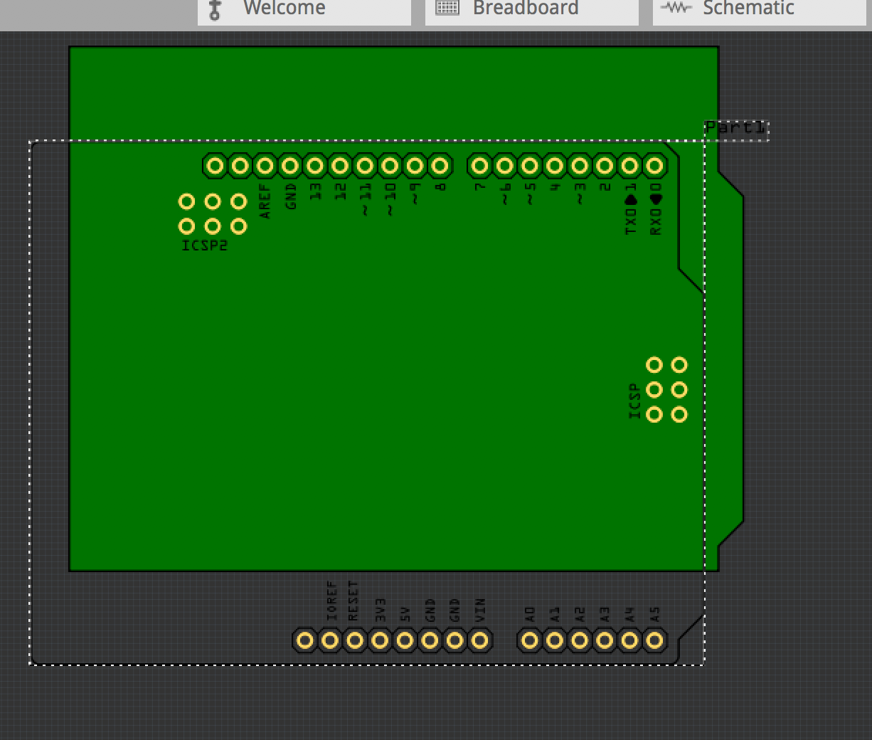
I have made a circuit board intended for use on an Arduino UNO.
The template for the PCB is square, is there an Arduino UNO PCB template to use that has the same shape as all the other Uno shields and the UNO itself? Mounting holes too.
There are UNO’s in the Parts - you can search for them (they are boards with stuff on them).
I made my own UNO PCB - I did not include holes as I don’t often use the standard UNO holes. When holes are needed, I use the “Hole” part and place them where needed.
Attached is graphic and files… You can use it/Hack it…
UNO_R3_pcb.fzz (1.5 KB)
The inkscape file - delete the fzz extension
uno_boardp.svg.fzz (1.6 KB)
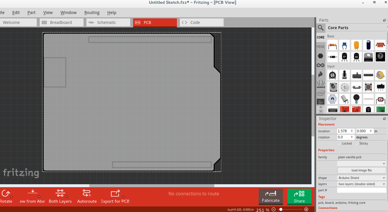
In PCB view click on the gray PCB that Fritzing starts with and then in the inspector where it says “Rectangle” you can change it to “Arduino Shield”. You do NOT need to make a custom PCB like opera_night is trying to get you to do.
Awesome!
Is there anyway to get the ICSP pins on there? 
Thank you both!
Nothing automatic. You could search for “generic” in the parts bin and then use a generic header. In the inspector you can change it to double row.
You can use the ruler to position the std header, like sub said, other wise you have to get the UNO svg and delete what you don’t want and import it into a new part.
1 Like
opera_night is it possible please upload the original svg with the mounting holes?
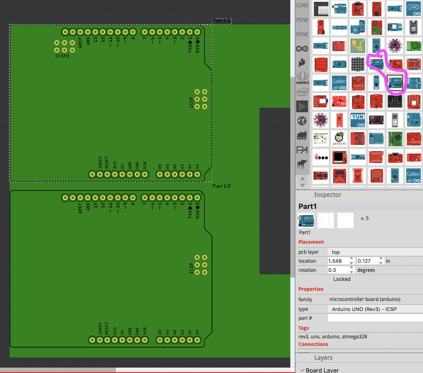
There are two UNO’s in the default parts bin (installed several yrs ago so, I don’t know about current installs).
In the search field at top of parts bin, enter Arduino etc…
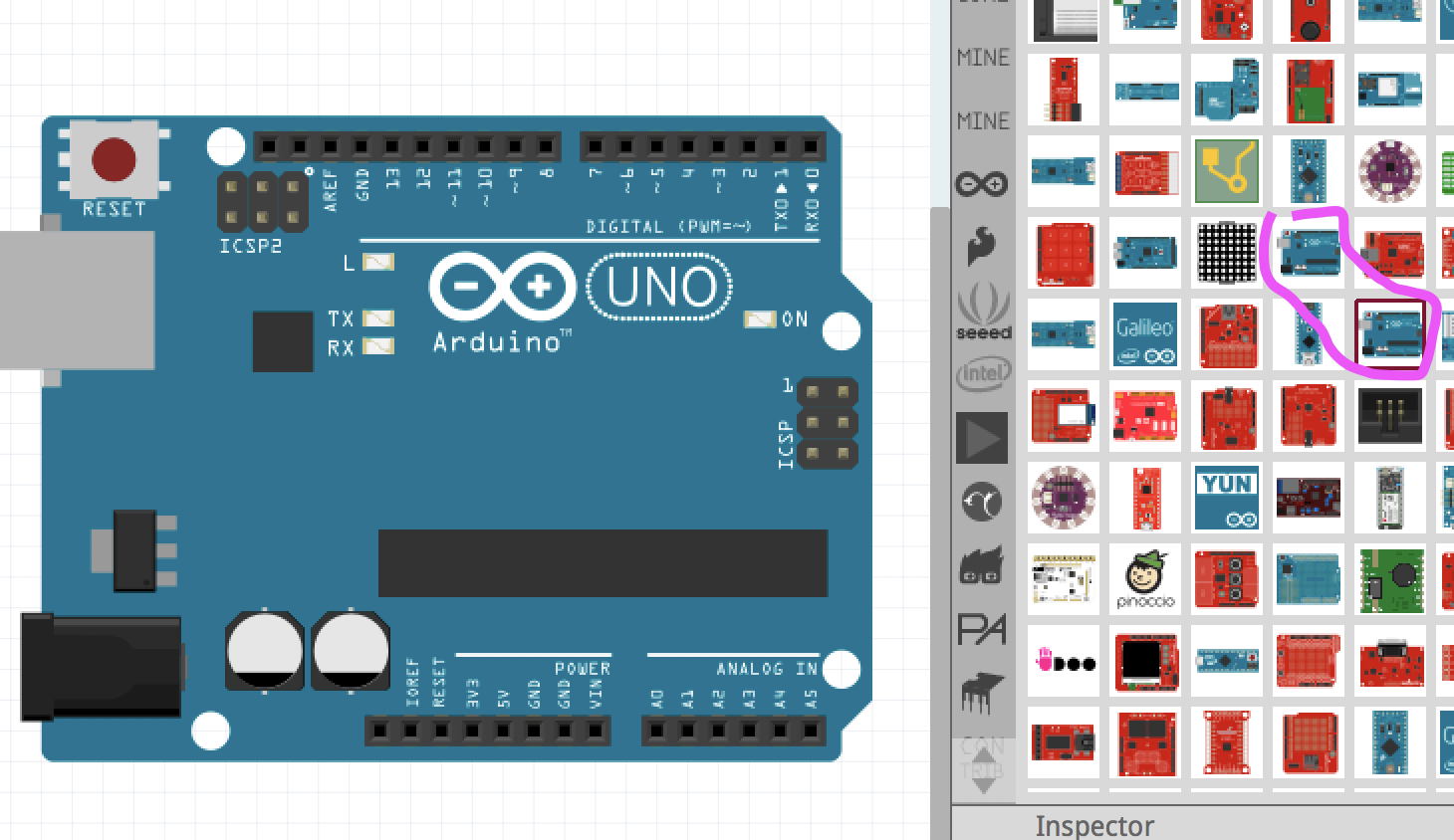
image below shows these two… one with iscp, other no iscp
I restored the file from backup but I’m not sure how to upload an SVG these days (site has changed)… Looks like it loads only as a graphic, not a file you can download…

The graphic image is fine. Just right click image in the post, save image as from the context menu to save it locally. In Firefox at least. Most browsers should work the same. Touch screen will be different. Probably touch/hold on the image until the menu comes up.
That image does not have any mounting holes. I thought jorge was looking for a version with the mounting holes.
Thanks - that worked.
Re the holes: Simply use fritzings Hole part, place them where desired.
Can get the placement position several ways:
• Physical measurement
• Use Fritzing’s Cursor position info (GUI panel lower right side, bottom)
• Drop onto the PCB the ‘Ruler Part’. Can rotate the ruler and can put in on the PCB panel, too.
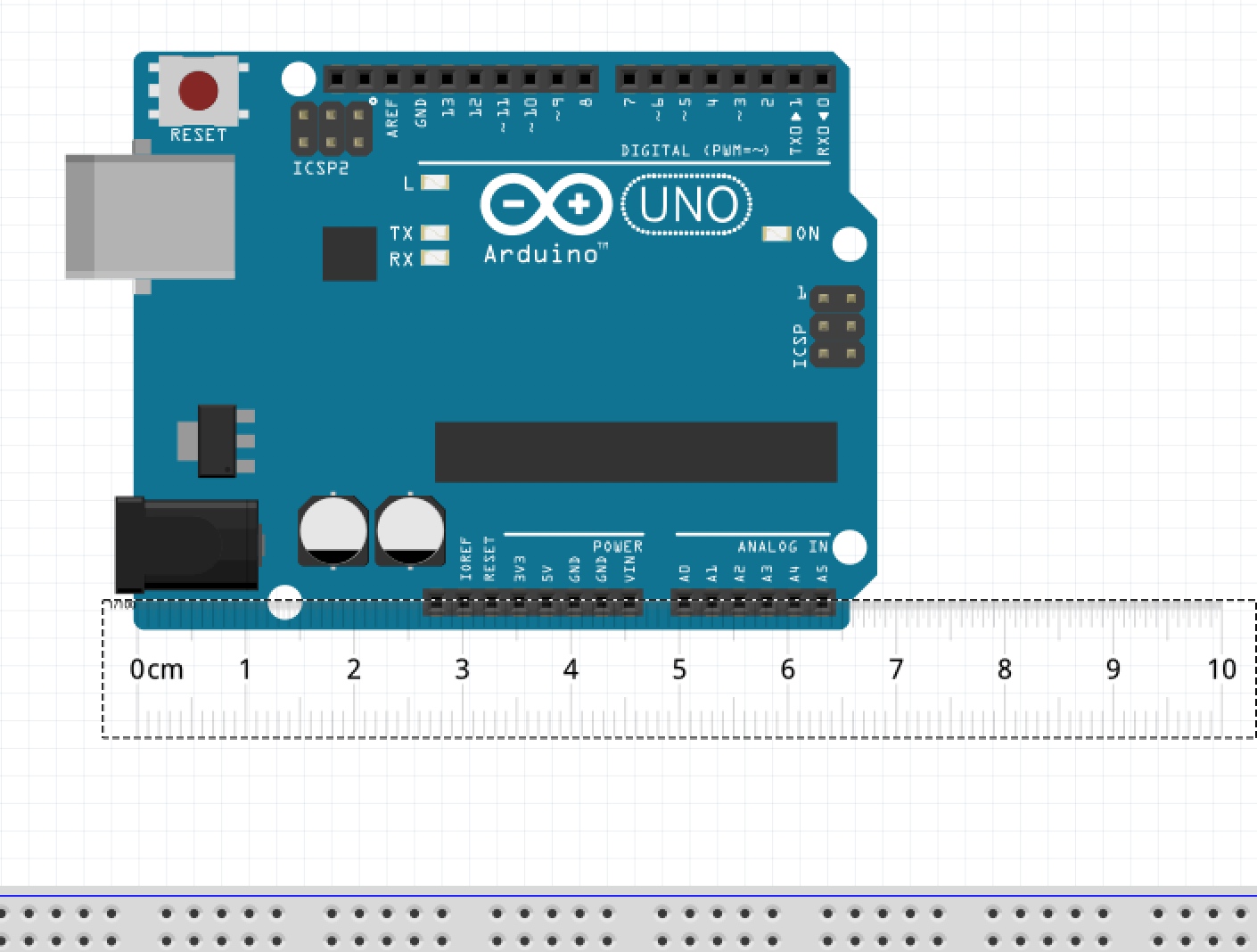
Image shows the SVG on top of UNO Part (offset to show the shapes more clearly)
Sure. The problem (for some users) is to get them placed accurately enough, relative to the headers, for a manufactured board to actually fit where intended.
I don’t use any of the methods you suggest. Instead, I edit the source svg file directly, and set coordinate values that way. Once I have the offsets from someplace else. It is not the UNO shape, but that is what I did for the pcb shape to create a part for a shield board. That worked, once I figured out the limitations and work arounds for Fritzing not handling some interior cutouts in the board shape.
Here is another process to get an outline, and holes, from an existing (breadboard) part. This works because usually the board shape and holes are a single path element in the svg file.
Create a new part from the existing part, export it, unzip the .fzpz file. That gets the separate part definition and svg image files for the part.
Delete everything from the breadboard image except the board outline shape. That can be done various ways. With Inkscape, select all, ungroup, deselect the board outline, delete. Might have to repeat, depending how the original part graphics are grouped.
Being familiar with the xml and svg file structure, I just use a text editor, search for the board outline path element (usually big, usually the first in the file), and delete everything else. The result of that is below. That contains the board shape, plus mounting holes, plus holes for each of the header pins.

Getting rid of the head pin holes is a bit trickier. They are embedded in the path element along with the mounting holes. In this case it was easy in a text editor. The mounting holes were the first interior cutouts in the shape, so just needed to delete all of the closed shapes after the 5th (the board is one closed area, plus the four mounting holes). Closed shapes are strings starting with “m” and ending with “z” in the path. That result follows. This is exactly as accurate as the original part definition. No coordinates where changed.

Because some of the original board components extended beyond the outline (usb and power jack), that leaves unwanted empty space to the left of the board outline. The final cleanup is to load that into Inkscape, select the shape, change the x and y coordinates to zero, then in the edit menu change the page size to match the selection. Final result.

With variations in the tools used, this is something that many Fritzing users should be able to do themselves. It is just a matter of knowning where to get the pieces, and the steps to follow.
WARNING:
Because of a bug in Fritzing’s handling of board shapes when exporting to gerber, the above images will not work correctly for custom pcb shapes. Only the first mounting hole will be in the correct location. The fix for that, is to change those relative move “m” commands in the path, into absolute “M” commands. Initially I thought that changing to “M” and recalculating the move coordinates would be enough, but the svg file contained a mix of relative and absolute commands for the circles. I needed to create the hole cutouts from scratch. The image below, with possible colour change, should work as a pcb shape, and create the correct hole cutouts when exported to gerber.

TLDR. From memory the holes are there in the PCB svg, just that they are in silk group. I think text is also in there somewhere. I think they hid them so it wasn’t as busy. I don’t know about the BB view.
The pcb view I looked at (others could be different) did not have either the holes, or the outline. Just the header pins. If a pcb view contains both the outline and the mounting holes, that would be a simpler place to start with this process. The extracted svg would have a lot less to delete, and the path would probably be correct for the gerber export. Though the outline might be only a “line” not a filled shape that would be needed for a pcb shape. The holes might be separate too, instead of embedded in the shape. Would need to check. I’ve used the breadboard view image before, for similar cases, so I knew (well was pretty sure) it would work.
Under silkscreen0 they are circle2, 4, 6, 8, just that they have white stroke and no fill. The plain silkscreen group has all the parts and text, it’s just turned off or all made white. It’s probably the whole BB svg, but with everything hidden. The UNO in my Arduino bin is like that, and my MEGA2560.