How to Make Capacitive Touchpads in Fritzing

Capacitance Sensors

Capacitance sensors detect a change in capacitance when something or someone approaches or touches the sensor.

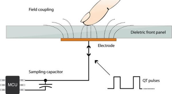
The electrode of a touch sensor represents one plate of such a capacitor. The corresponding 2nd plate is represented by the environment of the sensor electrode (to form a parasitic capacitor C0) and another conductive object, like a human finger for example (to form touch capacitor CT). This capacitor, i.e. the sensor electrode, is connected to a measurement circuit. The capacitance of the sensor pad is measured periodically. If a conductive object approaches or touches the electrode, the measured capacitance will increase. This change is detected by the measurement circuit and converted into a trigger signal.

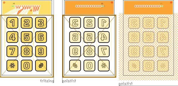
Part 1: Making Capacitive Electrodes from Copper Fill

In this example I will illustrate on how to make Capacitive Electrodes from a single PCB object or a combination of objects using Copper Fill.

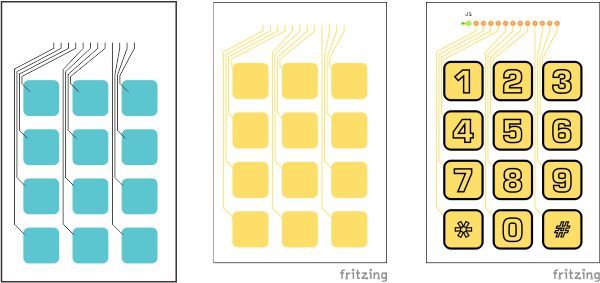
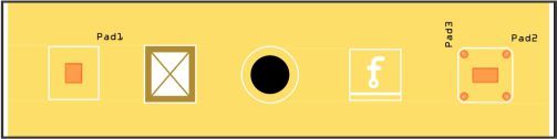
An electrode is simply the patch of conductive material on a substrate that forms the sensor. Common shapes are filled disks, squares and rectangles.

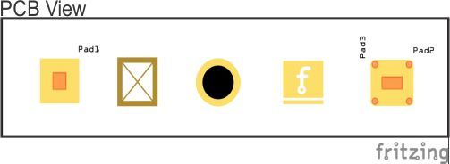
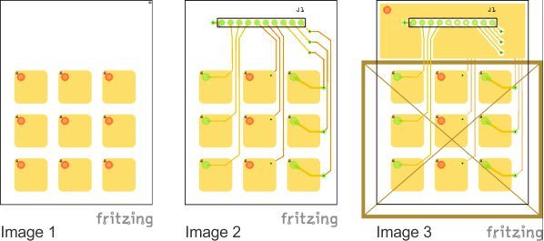
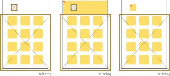
Step 1: I have placed five objects on the PCB from the Fritzing Core Parts (Solder Pad, Copper Fill Block, Through Hole, Logo Image, and the fifth one is made up of 2 - rectangle Solder Pads and 4 - Through Holes to give it rounds corners).

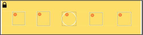
Step 2: I set the Top Copper Layer to Clickable only, then from the Routing Menu, I clicked Copper Fill (top), this will create a Copper Fill Template.

Step 3: I then locked the Copper Fill Template to keep the Copper Fills separated in the next step and deleted all objects.

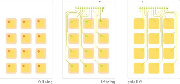
Step 4: , From the Routing Menu, I clicked Copper Fill (top), to create the five Copper Fill Electrodes. Each Electrode will have itā€™s own trace connector point, called Connector0

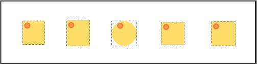
Step 5: Unlocked and deleted the Copper Fill Template.

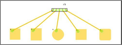
Step 6: Ran the traces from the Copper Fill Electrodes, Connector0 to the 5 - pin connector. These five Electrodes can all be used as Capacitive Touch Pads and will be covered with Soldermask from the fab house.

Reference:
Basics of Capacitive Sensing and Applications ~Texas Instruments~
Capacitive Touch Sensors ~Fujitsu Microelectronics~
The Art of Capacitive Touch Sensing ~Cypress Semiconductor~

3 Likes

Part 2: Making a Capacitive Touch Keypad using Copper Fill Electrodes

In this example, I took the Copper Fill Electrode that I created from the two Solder Pads and four Through Holes then made eight additional copies, arranging them in a keyboard pattern (Image 1).

Image 2: I placed a 10 pin connector and ground via on the top of the board, set the ground seed, and ran the trace. To illustrate different trace routes I created three examples; In the left column I ran the traces direct to Connector0 on the Electrodes; In the center column I connected the traces to a via in the Electrode; In the right column I ran the traces from the Electrodes Connector0 to a via).

Image 3: I Locked the nine Copper Fill Electrodes so they will not be deleted during the ground fill process. Placed a Copper Fill Blocker over the Electrodes to keep out the Ground Fill from around the Touch Pads. From the Routing Menu, I clicked Ground Fill (top), to connect the ground seeds to the Ground Fill copper.

Image 4: From the Inspector, I moved the Copper Fill Blocker to the Copper Bottom layer, as you donā€™t want a solid copper ground fill on the bottom of the board under the Touch Pads. I switch to ā€œView from Belowā€ and ā€œBottom Layer Clickableā€ only. From the Routing Menu, I clicked Ground Fill (bottom), to connect the ground seeds to the Ground Fill copper.

Image 5: Added the graphics to the Silkscreen Layer.

Image 6: A Gerber file image of what the Capacitive Touch Pad would look like from the fab shop.

1 Like

Part 3: Making a Capacitive Touch Keypad using Images

To be continuedā€¦

In Progressā€¦

In Progressā€¦

Making a Capacitive Touch Keypad using Images and Copper Fill

More to comeā€¦

Reference:
Adafruit MPR121 12-Key Capacitive Touch Sensor Breakout Tutorial

Part 4: More on Capacitive Touch Pads???

Making Buttons, Sliders, and Wheels in Fritzing

To be continuedā€¦

More to comeā€¦

Reference:
Buttons, Sliders, and Wheels ~Atmel~

Part 5: More on Capacitive Touch Pads???

Putting it all togetherā€¦

Capacitance sensors are an emerging technology for human-machine interfaces and are rapidly becoming the preferred technology over a range of different products and devices. Capacitance sensors enable innovative yet easy-to-use interfaces for a wide range of portable and consumer products. Easy to design, they use standard PCB manufacturing techniques and are more reliable than mechanical switches.

Easy to make - Simple Circuitry:

To be continuedā€¦

More to comeā€¦

Reference:
Capacitive Sensing Library by Paul Badger ~Arduino Playground~
QTouch 12 Channel Touch Sensor IC ~Atmel~

1 Like

Hi Iā€™m trying to make a specific triangular copper pad for my fritzing project that involves capacitive touch. The pads need to be a very exact shape and size and I canā€™t seem to figure out the best way of doing it. I have tried various ways;
ā€¢ The masking copper fill technique you have described ( but these came out rounded and pixel jagged and a different size to the starting shape )
ā€¢ Just making an svg and importing it as a logo to set in the copper layer ( But then you donā€™t have connector handles to run traces to it )
ā€¢ Creating a custom fritzing part ( but then these canā€™t be placed in the copper layer.
Any thought of ideas?

Do you want the solder mask over the top of your shape or bare copper? Do you want it connected with a trace on top or via?

Iā€™d like a solder mask over the pads if possible but I also need to be able to connect from both layers. For my first prototype I used the standard rectangular copper pads that come in the fritzing core and you can resize them. These you can run traces to and also drag the vias onto for rear layer connections. Iā€™m not sure if they have a solder mask on them, I mea they are shiny metallic so Iā€™m guessing not. However, I really need to be able to make triangular versions of these, which is why Iā€™m coming to you for help.

If the copper is a connector, you will not have a solder mask on top and not re-sizable. If you place it as a logo (image), a solder make will be placed on top and they can be re-sized.

Try this: place your image as a logoā€¦ place the connector that connects to it on the board. Draw a trace between the connector the will be connected to your image and some other connector (any connector), doesnā€™t make any difference. Now, put a bend in the trace and delete the section on the trace form the bend point to the other connector by right clicking on that section and select "Delete Wire up to bend point. Now you have a trace that goes nowhere. Click your mouse on the the end where the bend use to be and drag it on to your image. You should have a completed circuit to your imageā€¦ but the connector will not turn green.

Copper is copperā€¦ what ever appears on you drawing will be etched on your PC board.

Thanks. Does this apply to vias as well? Can I just put a via onto a silkscreen image thatā€™s in the copper layer and expect this to turn out like a pad with via in production? You say ā€˜what ever appears on you drawing will be etched on your PC boardā€™, does this also apply if Iā€™m not etching it myself but sending the gerber files to a pcb house?

Yes, you donā€™t need to run the trace to the imageā€¦ you can place a via through the image and connect to the bottom side of the via. But, a via is a connector and around that via there will be no solder mask. Although it is not that visible and probably not make any difference. You could place them all in the same corner to make it symmetricalā€¦ You could also place the via right next to your touch button and run a short trace to the image the way I had explained, then run you trace on the bottom side form the via to the connector pin.

Yep, copper is copper, DIY or fab house, it should be the same. You should check you gerber to make sure everything is connected and the solder mask looks the way you want it to.

Thanks for this advise. Iā€™m using a combination of the fritzing core pads and the improvised triangular ones we discussed above. How can I ensure the solder mask covers both types?

By using a gerber viewerā€¦ some people us the Gerbview in KiCadā€¦ there are several online ( http://svgerber.cousins.io/ and http://gerblook.org/ ) are just a couple. Your fab house may also show a gerber view before purchasing. Here in the U.S, I use OSH Park ( https://oshpark.com/ ) as both a gerber viewer and to purchase my boards. You get 3 board for $5 per sq/in, free ship world wide. Just check out the solder mask view. I always take a close look at all the gerber views before purchasing to make sure everything is correctā€¦ Sometimes your drill holes donā€™t come out as expectedā€¦ check those too.

Thanks for suggesting the gerber viewers. Iā€™m concerned because none of the holes are showing up, this includes the vias and the through hole components. Any ideas why this would be happening?
Also, how would I go about forcing the copper capacitive touch pads to have a solder mask on them? The self-made triangular pads do have the solder mask, but the pads from the Fritzing core parts do not. Is there a way of adding to this layer manually?

The Fritzing pads are connectorsā€¦ and all connectors do not has solder mask on them so you can solder to them. You would need to replace the Fritzing pads with your own custom pads.

Are your holes not showing up in the gerber view or the Fritzing IDE. In Fritzing, the vias will sometime hide behind other objectsā€¦ but the holes will still be there and show up in the gerber drill file. You can always send me the .fzz and I can take a look at it.

Ok, thanks, Iā€™ll replace the pads with the same technique of inserting an svg image as a logo object and putting into the copper layer. Will these still be the same thickness and work as well with capacitive touch (MPR121)?

With the holes, Itā€™s basically that they are not visualised in this 3D gerber viewer : http://mayhewlabs.com/webGerber ā€¦ but when you load one of their example boards you can see through all the vias and holes. Perhaps Fritzing outputs a different Gerber file name convention that Eagle?

Copper is copperā€¦ If it is a 1 mil copper board then all copper on the board will be 1 mill thick.

Gerber viewers are weird, they all work a little different. Try looking at the board in Fritzing from the back side or hiding the front copper viewā€¦

Great thread, I will have to try this outā€¦

Just to be clearā€¦ Can I do the following :

ā€¢ import an SVG into the copper layer to form my pad shape
ā€¢ place a via on top of this copper shape and another off of it somewhere
ā€¢ connect a trace from some part to both vias in series
ā€¢ select the first via ( on pad shape ) and ā€˜convert to bend pointā€™
ā€¢ select trace between bend point and the remaining via and ā€˜delete wire up to bend pointā€™
ā€¢ delete obsolete via

Basically what Iā€™m asking is; does it matter that Fritzing doesnā€™t know that I am connecting to the SVG pad shape? They are on the same copper layer and appear on top of one another, but Iā€™m not sure how this affects the creation of gerbers and the subsequent pcb fabrication.