Hi there so this is my first post here, I have made a few circuit board designs and need help vetting and making sure they work before i send them out to be produced, also would like feedback on the general design of them.
its a bit of a multi level design approach i am taking , there is a base mosfet switching circuit design that gets plugged into a “motherboard” that you then connect an esp32 to control the lights/dynamixel servos.
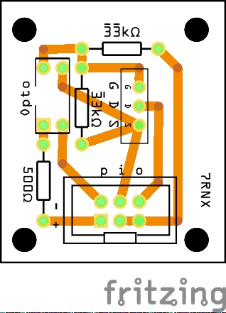
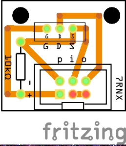
the design gets quite complicated, so ill start small first : the base mosfet pcb design :
small note P I O , stands for PWM , INPUT , OUTPUT
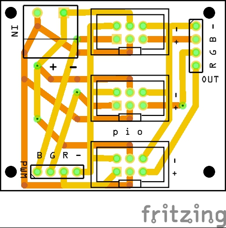
with this board you are meant to plug-in the previous board design , the input area handles 36vin , this breakout board can be quite useful for static theater lighting which is what i may use it for. let me know if this design seems sane !
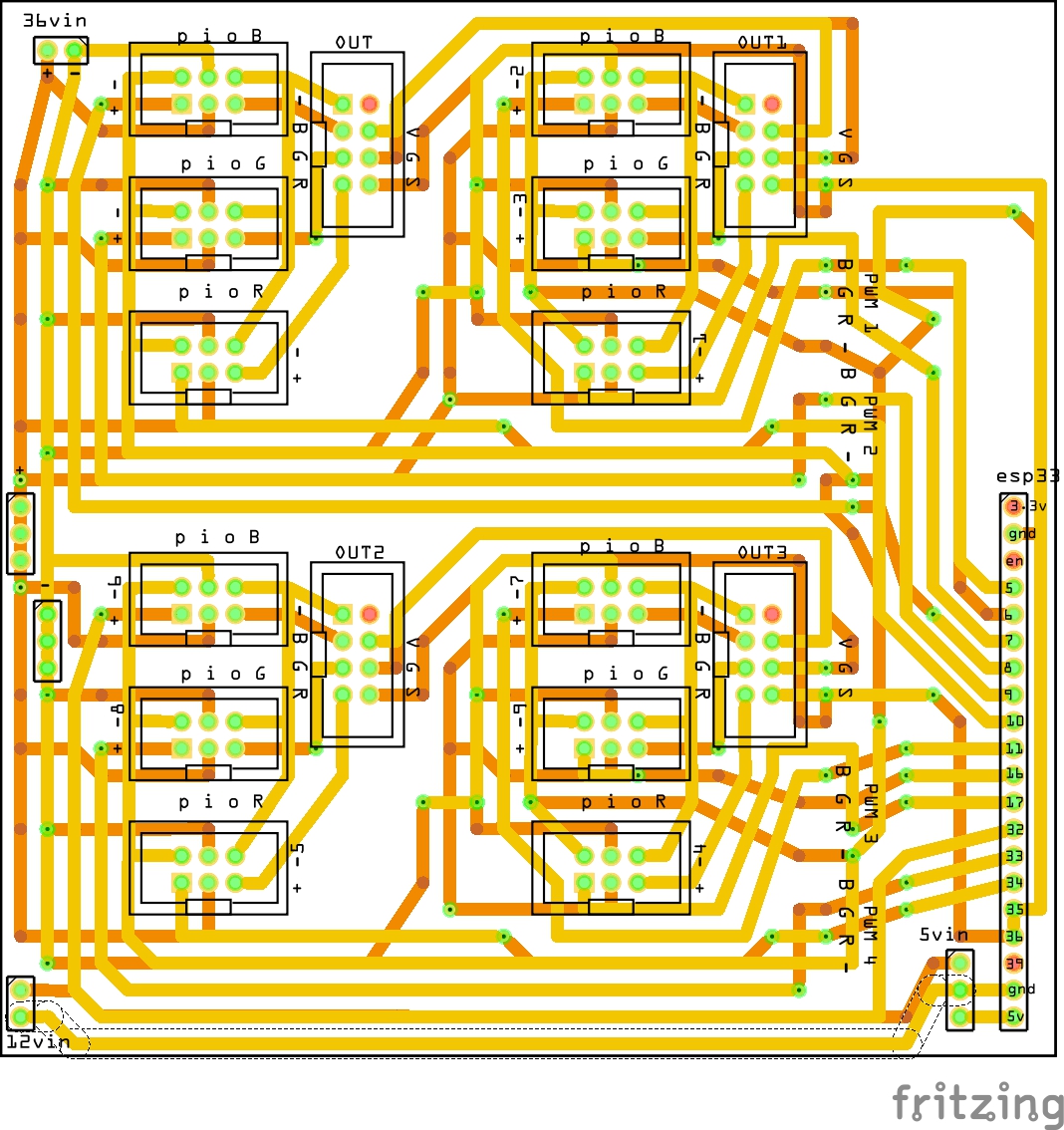
I had a few more tests like an esp32 breakout board based off the esp32 gateway card, but i think i am going to go write into the extremely complicated 4x robot light board design as that is the one that is giving me the most trouble. i think its designed properly but i am not sure.
note , i had to use a lot of overlapping lines to fit everything into 100x100mm so it may look confusing from the top. i was actually wondering if there is any way to have a special viewing option in fritzing so that when top bottom lines intersect they blend to make a different color?
the 12vin is from a buck converter that is fed externally by 36vin not on the board, also the 5vin is small non regulated dc/dc converter that fits that 3pin area.
I expect more information is required to give a good answer here, but I already see a number of problems. You say “high power” but the 36V power to the Mosfets are going through multiple .1 connectors (which are speced at 3A max but I would say even 1 A is likely pushing it). The mosfet gate is being driven from an optocoupler from a high resistance voltage divider which isn’t low enough (as it will give about 18V on the gate which is speced at 16V max with the swithing threshold at 2.5V so way to much voltage no where near enough current for good drive. I’d suggest a drawing showing how this fits together, this board with the leds (with their current draw specified) connected where you expect and the driver that drives this board so we can make better suggestions. Off the top you likely want high current screw terminals connected directly to the Mosfet source and drain with large wide traces and a much better drive circuit than is currently present.
On your last board above, the Design Rules Check
pcb view routing->Design Rules Check is flagging multiple overlaps that you need to resolve one way or another.
First off , thank you for that design rule check !! really helped out a lot. Second off , please forgive any current and future ignorance. First time posting here, first time even asking for help on this stuff
now to the first board, a little more explanation :
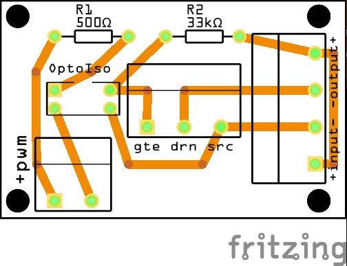
initially based off of this design, its an attempt to make the whole thing smaller and also to put in an optional volt divider for the mosfet due to the vgs being way too high for the mosfets we were using :
it is powering a 100w rgb led , each channel is one of those small mosfet circuits , so they are handling between a 26v and 36v input at around 900ma.
I will try to draw up some more details to more properly explain the whole scheme. for now maybe the current answer can address the first circuit board design?
Sure, mosfet gates are high capacitance. The implication of that is that it is an rc circuit and without sufficient drive a square wave applied to the gate rises slowly leaving the mosfet in the linear region where it has a high source drain resistance (since it is not fully on or off) and thus creates heat. What you want is for the Mosfet to be fully on or fully off as fast as possible. In your circuit the low state is fine, the optoisolator (assuming sufficient drive) drives the gate to ground quickly through the collector of the output transistor. The high state is currently a problem as it is 1) to high a voltage for the gate (18V against 16V max and 2.5v threshold) and 2) the gate capacitance is charging through a 33k resistor and thus will likely have a slow rise time. Whether that matters or not depends on how much current you are driving. If the output current is small it probably doesn’t matter, but if you want to drive 3 or 4 amps it likely does. The issue is power limits on the mosfet. The cure is to provide higher current drive in the high direction.
Given that this is a logic level mosfet, the easy way to achieve that is to use an optoisolator with a totem pole output. That drives both high and low with a transistor (providing a high current spike to charge or discharge the gate capacitance,so you want to add a bypass cap on the power supply at the optoisolator as well). The downside to that is that you would need a 5V power supply (a $2 ebay buck converter from the 36V supply to 5V would be my choice, although 36v may be above their input voltage range too) to drive the optocoupler VCC lead. That needs a position on the connector which is often an issue but in this case you seem to have one. You can also, with some tuning, use a capacitor (the value of which needs to be close to the gate capacitance) across the resistor to the 36 volt supply to supply the needed current spike to charge the gate capacitance but the active driver is usually easier to implement.
vanepp , wow , lots of words that i will have to research to understand hah, thank you for the input and hopefully i can get back with a better design.
question though, where are you getting the 16vmax and 2.5v threshold numbers?
From the mosfet datasheet for the stp16nf06 which is the mosfet part number in your sketch (which is what I assumed you were using, perhaps incorrectly).
that or the data sheet for the device you are actually using will give you the limitations. In this case in absolute maximum ratings Vsg +/-16V (meaning don’t use much more than 10V to stay safe) and further down under On Vgs(th) min 1V max 2.5V which says that with more than 2.5V on the gate the device will be fully conducting (although the threshold graph later says that’s a lie, as you need about 5V on the gate for full conduction at 28 amps.
the main flaw with this design is the esp32 outputs a 3.3v pwm instead of a 5 or 4.5v pwm so the totem-pole opto sounded interesting as that might amplify its output to the required 4.5/5v ?
also heres the data sheet for the mosfet i am currently using , the input voltage is 26-36v and the max amps are about 900ma
With a 1 Amp load and that mosfet it is likely your initial circuit will work fine. That mosfet has a ±/30V gate breakdown so 18 volts isn’t a problem and at 1 A it is way under utilized and you aren’t likely to see any problem related to switching speed. It only becomes an issue if you are switching large currents (6 or 8A say in the original mosfet) that will cause heat in the mosfet if the switch isn’t fast enough. I’d still consider running the output to a connector directly on the board where the mosfet is rather than through other connectors, as each connector reduces the reliability of the connection.
Peter agreed , that is what that giant motherboard design is for, the small mosfet circuit plugs into that, there will be 12 of those small mosfet circuit cards going into the mainboard. for outputs on the mainboard, there are 4 and each output handles the - r g b of the lights and also the volt ground signal of the dynamixel ax-12a servo.
good to know the initial circuit design should work , i will keep trying to understand more what you said as improvements are always good.
Remember that current is additive, so 12 loads each of 1 amp imply that there is 12 amps flowing in the ground connection at the point they all come together (assuming a single 36V power supply). That means that point has to have large gauge wire and high current connectors. It can also cause ground offset problems for the logic, but that is what your optoisolators are for, to isolate the logic ground from the high current ground (which it sounds like will be your mother board which may or may not be able to handle it). The servos look to be capable of wanting another 1.5A each at stall so that needs to be figured in as well.
those traces are the biggest ones that fritzing has, if you notice in the Mboard design , i have a line of 3 inputs on each of the positive and negative of the 36v in (technically 8 with the top two inputs). i will be using a 500w 36v power supply and am basically taking all 3 of its outputs and connecting them all at those two middle input points, i was however thinking that maybe i should try to have a few more traces coming out to spread all of that power around but havent done so yet as the circuit trace puzzle was too strong atm.
also, the 12vin will be connected to the 36v externally and will supply to the ax-12a servos, i will probably have to find a slightly beefier buck though as the one i currently have only does 8a max.
Will probably need a 600w power supply for this as its 400w of light + 144w of servos , 544 watts damn , thanks for spotting that (just double checked the data sheet)
You may want to ask your board house about extra weight copper. I believe you can get heavier weight copper for high current applications for an extra fee. There should also be a calculator around on the net that will calculate needed trace width / copper weight for various currents. I rarely make boards so I’m not the one to ask. Hopefully one of our board aware folks will comment. Splitting the 36 volt supply in to three feeds is a good bet. That reduces the current density in any one path which is valuable and/or allows smaller trace size. The feeds in to the board need high current connectors of some type. You may end up with ground issues on the servos too. If they are like usual servos the ground for the motor and ground for logic are the same, but with many servos and high current it doesn’t take much to get a ground offset of .5 or 1 volt which will affect the logic drive of the servo. The preference is to have one wire to the servo motor power source and another wire that goes back to the ground on the logic (out of the high current path and thus hopefully not affected by high current voltage drop in the grounds) but you have to be careful of ground loops in such a situation. You may end up needing optoisolators for the servo control leads too.
That is not the biggest traces, just type 128 in to the trace thickness in Inspector. You can also add extra solder on those traces to increase their capacity. Find a track thickness calculator online.
