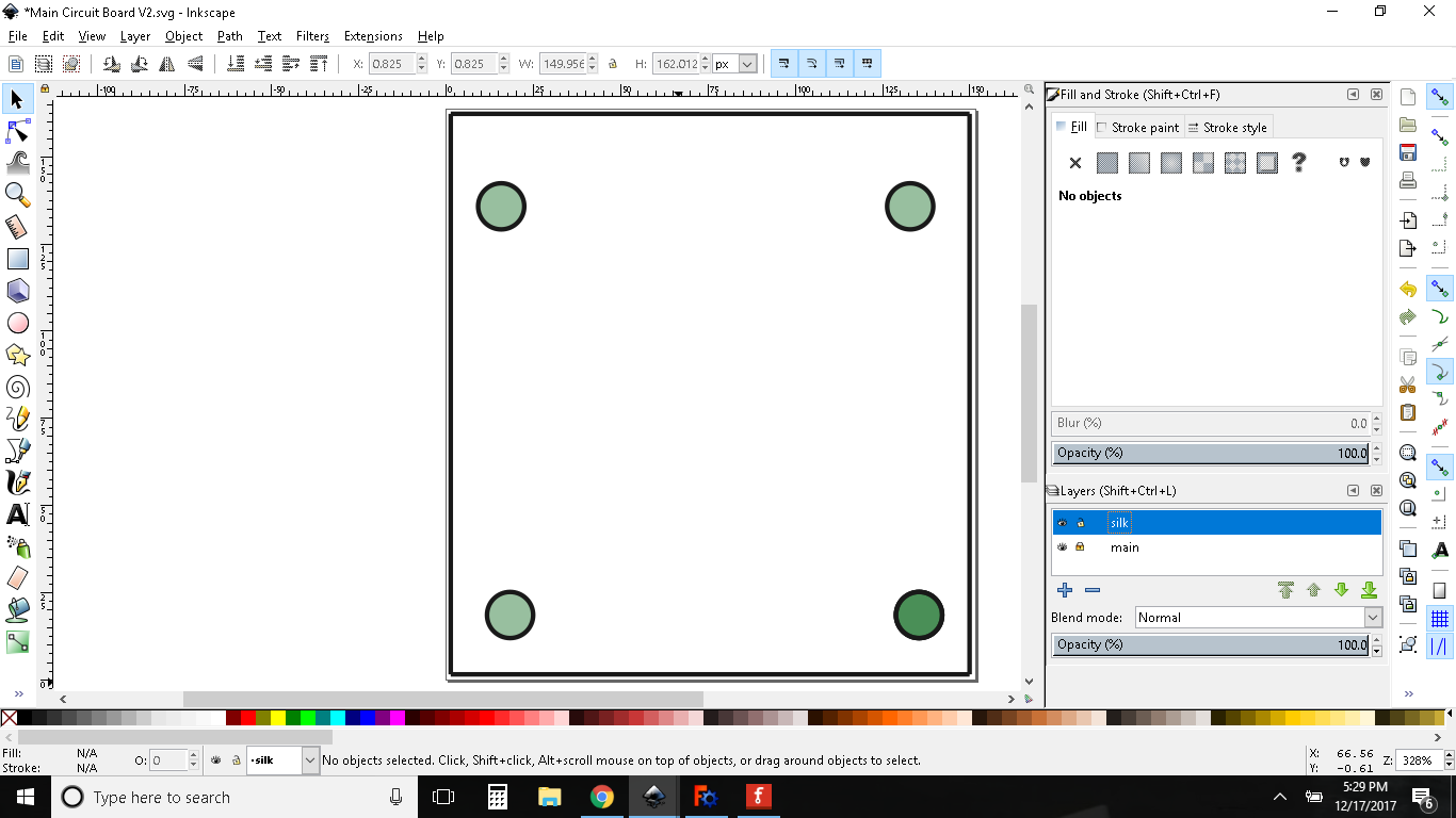
I’ve been trying to create a custom PCB but am stumped very early into the project. As you can see its just a simple rectangle with 4 holes in the corners. I created the board in Freecad and exported the file as a SVG. I have been following this guide (https://github.com/duff2013/Fritzing-Custom-PCB-HowTo) which has been great so far. When I add the color it is coloring the holes in the board. Not the board.
Assuming this is Inkscape (as it looks like), you need to select the board via (assuming the board is part of a group) cntrl-left mouse click. With the board selected, clicking on a color in the bottom color bar will change the fill (and thus the color of the rectangle) to that color. You can also do it by using the xml editor and changing the value of the fill command in the style section (but the gui in this case is easier). That brings us however to the question of what are you trying to do? If this is a pcb, you normally wouldn’t be putting a color on the base, you would be adding copper traces and silkscreen (usually via Fritzing rather than FreeCad). If you are making an svg for breadboard view, then indeed the above instructions are correct.
The only purpose of Freecad was to create the shape and holes in a custom shape PCB. I did what you suggested and highlighted my shape and chose a color which only colored the holes. Not the board. According to the example I am following, Fritzing needs to see a certain color to work. I was under the impression I was only making the shape and silkscreen of the board in Inkscape. Fritzing will be making the traces. As you can see I have two layers. The Main board and silk screen.
Custom board shapes is a bit out of my experience but silkscreen layer is usually black (that said, Fritzing doesn’t care, any color will be converted to black in the svg, the import mechanism however may care in some way I don’t know). It does however care that the layers are correct in the svg and you need to get your constructs under the silkscreen layer group but the import process may deal with that too. Which set of instructions are you following and I will have a look at them.
Edit: probably your best bet is to upload a copy of the svg here. The forum often doesn’t like uploading svgs, so the best way is to rename the .svg to .fzpz and upload that and tell us that it is really an svg. From one of the other posts on board shapes I found your groups are likely incorrect.
That said if all you want is a square board with mounting holes (as opposed to a fancy shape) there are easier ways to achive it (dragging the hole from core parts pcb for instance)
Fritzing likes the board svg to be very specific. Since you created it in Freecad you will need to break apart the svg and then do a difference to create the holes. To do this in inkscape select all (ctrl a) and then break apart (ctrl shift k). Now select just the parts you want as holes while holding shift (you may have to be in node editing F2). Then merge them with a union (ctrl +). Now you should have two parts. The board and the holes. Now select both of them while holding shift and do a difference (ctrl -) which will cut out the holes from the board. You must do the difference last. If you move any vertices after the difference you have to break it apart and do the unions and difference again as the order the vertices are defined in the file matters and Fritzing will not be able to make the hole in the contour file.
You also need to have the group ids set correctly including case.
board not Board
silkscreen not Silkscreen
silkscreen0 not Silkscreen0
Board and silkscreen color does not actually seem to matter at all.
I’ve tried using the hole in the core parts but unless I’m missing something it’s difficult to place them in specific places. 31mm between holes. 4.5 mm from left of board and 4.5mm from bottom for example.
I rarely make boards, so I’m not the best source, but someone lately posted (and which I now find I failed to mark and can’t find) a post on a way that I think allowed you to make such adjustments in pcb. Hopefully one of the pcb oriented folks will be able to point to that post. I tend to cheat in such cases (although not I admit on a complete pcb so far) and directly edit the underlying svg.
One way to get the hole exactly where you want them in the PCB view is to use the inspector. First you set the board to 0,0 which is the top left corner and then you set the location of the holes doing the math. So if the hole is 4mm and you want the hole centered 10mm from the left and 10mm down from the top you would set the hole location to 8,8 because it measures from the side of the hole not the center (distance - radius).
You also need to have the grid disabled to get them at exact positions.