I’m designing some cove lighting for a living room using a Raspberry PI and two addressable LED strips (WS2812B, 300 LEDs each).
I’ve got the lights and a prototype breadboard already set up, so I know the circuit works. What I want from this post is a sanity check on the circuit itself as well as any advice in making a better PCB. This is also my first time trying to make a Pi Hat.
With this project, I am trying to create a shield/hat in order to declutter as much as possible. I want to power both the LEDs and the Pi using a barrel jack so that I can avoid using the USB power cable.
My components are as follows. Apologies for the wonky links, I am still limited to 2 total links:
I am hoping that this part will work - I will need access to the GPIO pins for future switches:
h ttps://www.sparkfun.com/products/14017
I have a 5V/15A power supply that I am intending to use. I’m a little concerned about the possibility of frying the Pi with this much current (I think the hold current is 2.6A), but I don’t know how much a fuse would help me.
• I use only parts for which I have/use actual hardware. Thus, I replaced your connectors and power plug with parts I use, knowing they relate to my using them in Fritzing and on real boards I make.
(I’m not saying anything is wrong with parts you’re using)
• The Power-Plug you used appears to not have the pins in exact same location as the one’s I use (drop them both onto a new board and compare. Use the one you want…
• 90º Pin Connectors. I replaced yours with Pin-Headers (what’s important are the pads/position/thru-hole diam. These headers eliminate the green-pcb from the BB for a cleaner look)…
• I Repositioned the board so it overlays on the PI
• Tweaked the traces for straight and 45º (helps eliminate noise). Just an example of what to strive for…
• I did not re-attached wiring in schematic/BB
Although I have several PI’s, I did not pull one out to check location/dimensions etc…
Further considerations:
• Trace widths and routings
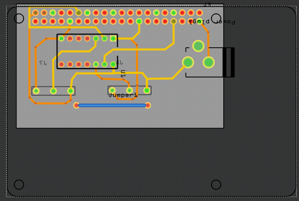
• The PCB could easily be made at home (or use perf-board as you show). It would be easy to make it Single-Layer PCB by adding a couple of Jumper wire parts - I put one on the board without hooking it up but, you can imagine how it would eliminate the Top of the board traces if desired
(look at my Motor board as example)
Your files with my above mentioned tweaks is attached: rpi_ws2812_shield.fzz (34.5 KB)
There is a fritzing part for the 74x125 (which is what the ADA1787 is) available here (I think I have been too lazy to submit it to core parts):
just download the fzpz file and in Fritzing File->open the .fzbz file will put it in the mine parts bin ready for use. As it stands your circuit is incorrect. The 74x125 is wired incorrectly. Pins 1,2 and 3 look ok (enable on pin1 grounded, input on pin 2, 5V output on 3) but pin13 is the enable and should be on ground, pin 12 should go to the PI as input and 11 (currently unconnected) is the 5V translated output to the LEDs. As well pins 4,5 and 9,10 need to be grounded as CMOS doesn’t like floating inputs. Finishing schematic would be a good bet as it makes problems like this easier to see. Then on to pcb issues. 600 LEDs are likely to want a lot of current and that needs reasonable care. The barrel jack you specified is only rated for 2.5 amps and the LEDs will likely want a lot more than that (the screw connectors are rated at 8A which also may not be enough, the originals are specified to 16 amps). Plan for the maximum current that all LEDs being fully on at once would draw. Don’t believe the “derate the current draw due to multiplexing” suggested on many LED sites as that only works with sync clocks and WS2812Bs have async clocks which will sometimes draw full current, so plan for it. The Fritzing barrel jack footprints have problems as well, I’d suggest replacing the barrel jack with a 2 position terminal block. It supports more current and the wires screw in which is desirable. That said your pcb layout needs much larger trace sizes and shorter routing on the power traces to the LEDs to deal with high current. You will likely get from that many LEDs. The power and ground traces to the 74hct125 should be separate from the high current path to the LEDs to avoid voltage drop issues and the trace width on the high current path want to be as wide as possible (consider using ground fill to use all the copper available) and as short as possible to avoid voltage drop issues.
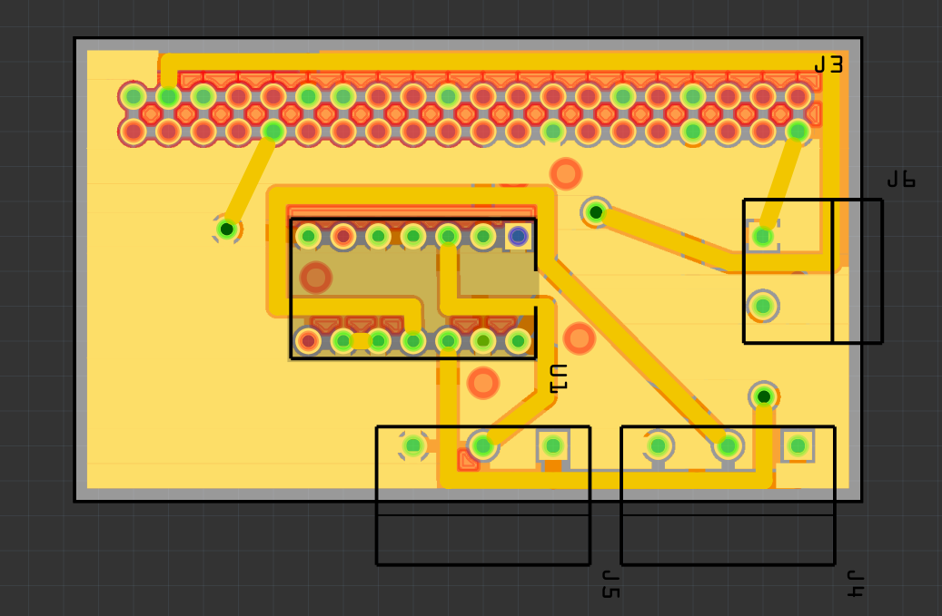
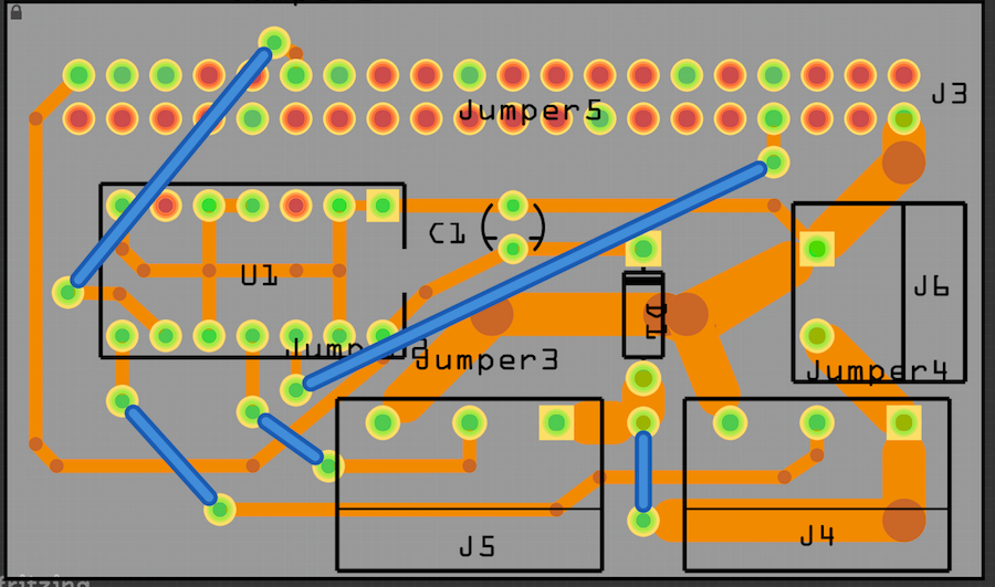
I’ve gone back into the project and tweaked the PCB according to my best understanding of both of your comments. Here’s the file: rpi_ws2812_shield_2.fzz (94.2 KB)
I’d link an image of the bottom, but I’m limited to 1 per post.
The major tweaks:
replaced the barrel jack with a 2 terminal block
replaced the quad level shifter with VanEpp’s 74x125
fixed the 74x125 pin connections
connected floating inputs on the 74x125 to ground
pins 6 and 8 are still floating
increased trace width
cleaned up trace geometry
repositioned the 3 terminal blocks to be closer to the power input
added a ground fill
Etching this at home sounds like fun, but I just want to tackle one project at a time. I’ve had this breadboard prototype setup for months and now I’m more concerned than ever that it’s a literal fire hazard. Next time though!
I decided to stick with the big terminals as well since it sounds like I’m going to need them. Each strip looks like it can draw 18A max. I’m now looking at these terminals instead of what I’d previously linked:
No idea where I should even look for a 40A terminal. Sounds like a total hog. I see some 5V/40A power supplies, but I’m happy to wait on that.
I’ll admit I’m at a loss as to the best strategy for separating the traces powering the Pi and the 74x125 from the LED terminals. Should I just create a new trace directly off of the supply?
I’m afraid I missed something… 18 Amps… 40 Amps! My Arc welder only pulls 14 Amps!
Your home’s wiring won’t handle 40A and no doubt, 18A will also blow breakers/fuses…
And, a PCB with thin copper traces… Go to Home Depot and look at the thickest wire (or extension cord) see what Amp’s they’re rated for…
I think you’re headed in a direction leading to ‘Death’… Please check again. You should only need a source capable of only a few amps, max. We’re talking LED strips aren’t we?
EDIT: Added…
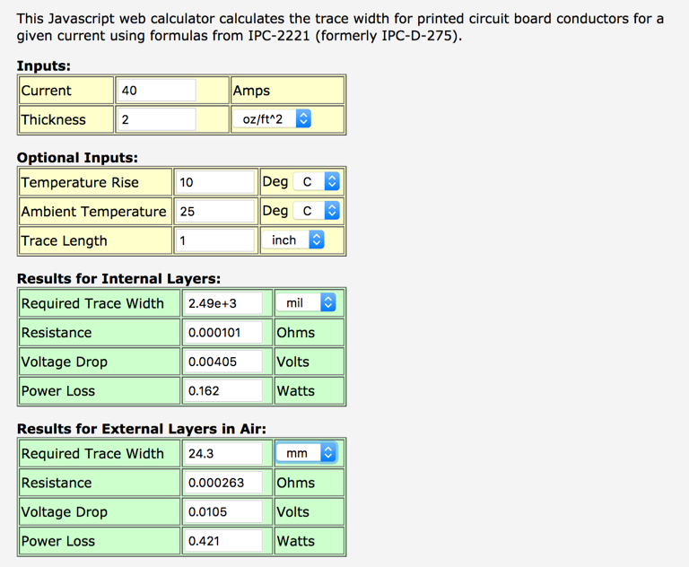
Typical results for calculation of typical PCB…etc PCB Trace Calculator
This shows for 40Amps, traces need to be 25 mm wide (on a 2oz board)…
EDIT: Thought this may help (looked at WS2812B data sheet). I think this should help your understanding more clearly than posts… Click the Data Sheet link to go to pdf for Raspberry PI
converted from perf board to a breadboard as I find making reliable connections easier. Ran power wires as they will be (and are) on PCB. The 2 pin connector that provides power is the base connection of a star layout. One line from the star (both power and ground) goes to the RPI and level translator. A Schottky diode and tantalum cap was added for 2 reasons: it isolates the RPI power source from voltage spikes caused by the LEDs drawing power all at once and if the USB is connected, protects the USB from trying to power the leds (the diode will block it), there isn’t such a diode in the RPI schematic I looked at. If a current spike drops the 5V line, the diode will block the LEDs from drawing current from the bypass caps on the RPI leaving it with a stable supply of 5V and avoiding software crashes due to undervoltage. That may or may not be needed but it is cheap insurance. In pcb view, there are separate traces from the 5V input pin on the 2pin connector to the RPI diode and both of the led output connectors. That way any current induced voltage drop in the high current traces (the power to the LEDs) only affects the LEDs not the RPI and the diode and cap should filter them out anyway.
Rather than do ground fill I cheated because it is possible to type in a number up to around 128 in to the trace width box in Inspector and get extra wide traces. In this case I used 100 as being about as large as is useful. You could use ground fill to do the same type of thing and I think @opera_night has some other tricks for creating large controlled copper areas in pcb (I don’t usually do pcbs, so I’m somewhat out of my area of expertise). The RPI connector has only one connection for 5V and one for ground to avoid ground loops. The multiple pins on the connector should have internal connections on the board and thus an external connection to multiple pins can form a ground loop. Finally I moved the connectors so the base of them are entirely on the board (you may have a reason for placing where they are and thus have to move them back though). The reason for this it to give them the maximum mechanical stability in the case where someone pulls on the wires connecting to them by accident. The more area supported by the board the stronger they will be. Hope this helps!
Remember this is at 5V not 120, so while the current is extreme, the power isn’t that severe. In his current project he has 300 leds, the referenced data sheet says assume each LED can draw up to 60ma, that means with everything fully on he is looking at 18A at 5V but only about 90W. He does however have to consider the current paths if he wants to be successful at this as that much current will produce voltage drop due to wire resistance, probably to the point where the LEDs ws2812s will stop working due to low supply voltage. Luckily the current is by strip, so you can run multiple power supplies and thus distribute the current draw to suit the situation by using more smaller strips and multiple power supplies, but care for high current practices on the pcb is still required.
Peter, yes, I saw he wants to use 2x300 led’s (and, at a max of 60mA, the math indeed, does calculate to rounding up at 40A).
BUT, the modules and code dictate PWM and duty cycle - thus, as you know, that mean much lower continuous draw.
My point (though not clearly stated but inferred via “… help your understanding…”) is/was to understand just how much Power/Current (at a Voltage) would be needed.
I also didn’t say (but, assume) understanding includes that, just like a Home capable of supplying high current at, say 120vac doesn’t mean a draw of 1A gets the full potential, Home supply’s capability…
Lot’s of stuff to know but a full discourse/more-clarity via posting isn’t my cup of tea, I guess.
Having cleared my plate of current projects and always looking for a reason to fire-up my CNC mill and make PCB’s, This is an Offer…
Once, the Single-Layer board design is completed, I’ll make a PCB and mail it (in USA). No Cost!
Constraints:
Max board size (so I can use my existing pcb blanks): 100x70 mm. Max circuit size: 80mm x 60mm (to avoid my needing to make a new board fixture).
It won’t have a silkscreen but, one can be printed from the Gerber (and transferred to the PCB via Acetone…) or printed on clear-print label products.
( why ‘Single-Layer’ ? Because: 1) that’s what I have in stock, 2) user would need to add Registration feature so when milling other side, the Vias, Holes, … line up…) Thus, use of Jumper wires…
Unfortunately there is an rc oscillator in each ws2812b that controls the pwm portion that is not synced to the data clock. So when enough of them drift in to sync at random (which apparently happens) large current spikes can occur. The code doesn’t have any control over this because of the async nature of the rc oscillators. Seems a design flaw to me (not syncing to the data clock to allow software current leveling) but there may have been constraints on asic size or cost that dictated, but it seems to work as long as folks prepare for the large spikes. I’ve only read of this, I’ve never used the actual devices.
Yes, agree with your comment. Personally, I would not use a PI.
(Oh, Arduino pins are 40mA but, can be ganged to one output line to provide multiples of 40mA. Perhaps not useful for this project but, good info to know).
Concluding my PCB milling info:
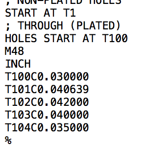
I should have added comment about Thru-Hole diameters and Pad size:
Many parts used in Fritzing do not have correct, consistent hole diameters - this causes Gerber drill file to list everyone, thus, un-needed pains for milling/drilling.
Drills: The solution is to use common-rounded drill dim’s. Ex, if Part A wants 0.87mm and Part B wants 0.11mm, I use 1mm drill.
Pads: Sure, I can do the default pads in Gerbers but, because of variations in milling (resulting in possible narrower/wider pads, I alway change the Pad shapes to Oblong (where possible). Thus, reducing potential for lost copper while increasing surface for soldering…
(It’s important to ensure the hole diam accommodates the Pin on the part (especially for square/rectangular pins). Thus, check the parts…)
Example: Some will be oblong, some won’t - depends on orientation…
I tweaked Peter’s updated file to make it a Single-sided board for Milling or Etching:
• Added Jumpers and widened traces (from 24 to 32)
• Shifted one connector to provide some space for a jumper
• Other tweaks are obvious…
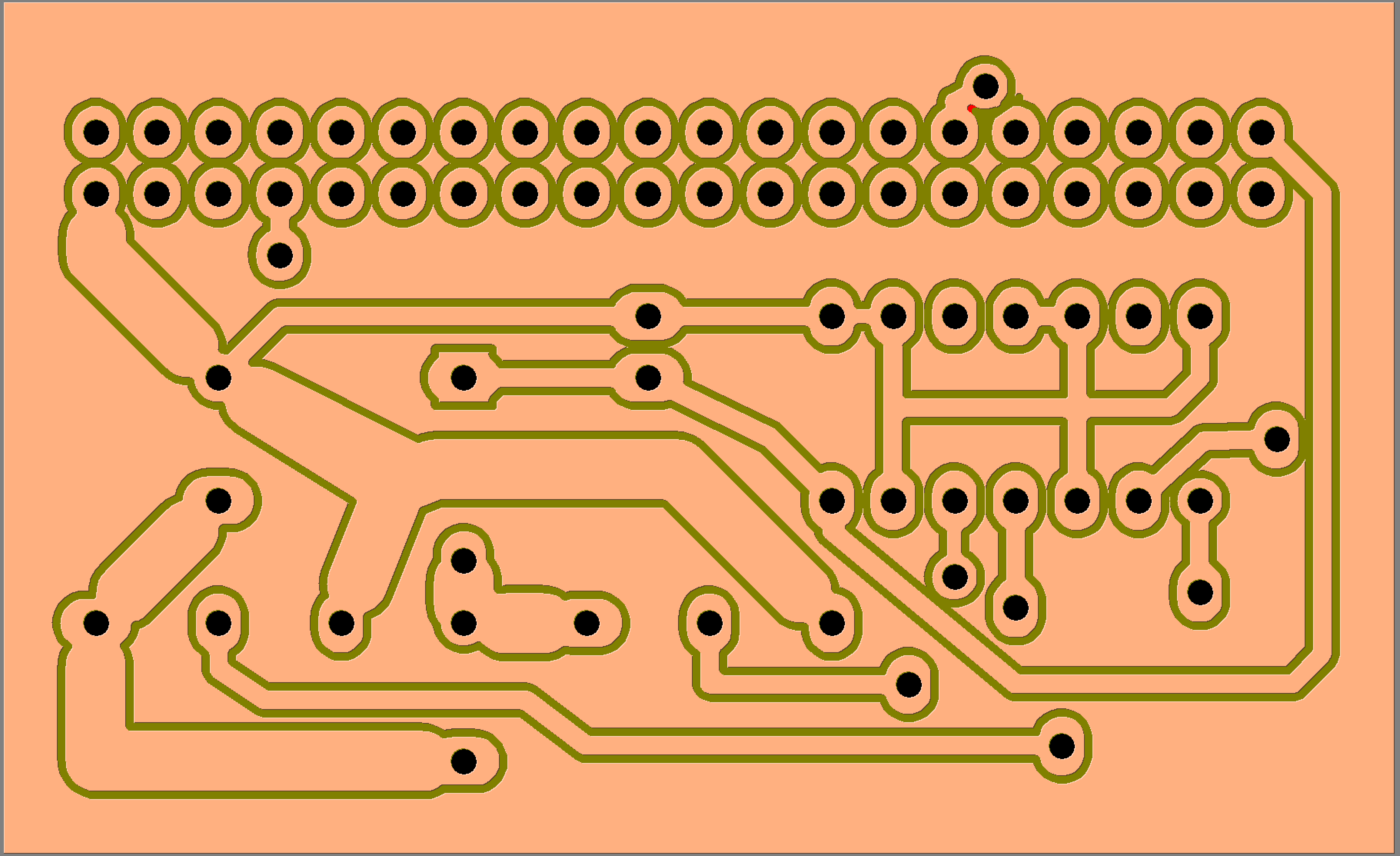
Note: As mentioned… (FYI) thru-hole diams vary from part to part and show up in the Drill gerber: You can see that common-sense suggests using a rounded-up diam for these 5 drills…
Lastly: Regarding Ground-Planes… Etching will remove all the surrounding copper (unless inked-up with Permanent Black marker). Milling will leave all the surrounding copper which can be bridged (via wire) to the Ground, thus creating a Gnd plane. It can be sectioned by cutting a slice with sharp blade…