Although my question isn’t really difficult i notice
it isn’t easy to do it in english
I searched whole internet but couldnt find a solution.
What i wanna ask is:
How can i insert a single copper connection like via on a pcb
(but NOT a via, cause pcb will be singlesided) ?
Think of soldering a wire on the pcb … i would drill a hole from the upper side of the pcb
and then there has to be a dot of drilledthrough copper on the other side where i can solder my wire.
Think of the endpoint of a resistor without resistor …
As i understand we connect parts, but what if there’s no part just the need to have a
place where i can solder and connect to other parts ?
You can post the question in German and we will use google translate to translate it in to English and ask if we can’t figure out the translation.
To do this (because it isn’t obvious how ), click on the grey board outline in pcb view, then in Inspector (the window on the bottom right) you should see PCB1 at the top. lick on layers, which is by default double sided. Change that (via the pull down menu) to “one layer (single sided)” and you have a single sided board. Then any of the suggestions above should do what you want.
Hi again , happy easter and stay healthy everybody
The solution i asked for was the suggestion from opera_night.
I was happy with it until i began to think about printing the parts layout to the non-coppered surface of my pcb. The printing question is/was discussed in another thread and the suggestion made there will lead to a satisfying solution - i hope
Back to “copper dot” i use now - it is a single pin header,
which in reality is used when a simple wire has to be connected to the pcb.
Works very good when i develop a pcb AND when it comes to the solder part.
When (in near future) i print the parts layout there’s one thing which i really don’t like,
the pin header is symbolized as a square (which is obvious as it is the shape of the pin header).
But, and this is where i need help, i don’t want to print the sqare,
cause for me it’s a soldering point/dot simply said.
I tried to edit the pin header with the parts editor thinking that there must be a
possibility to delete the black square … but there’s none
(or i can’t find it).
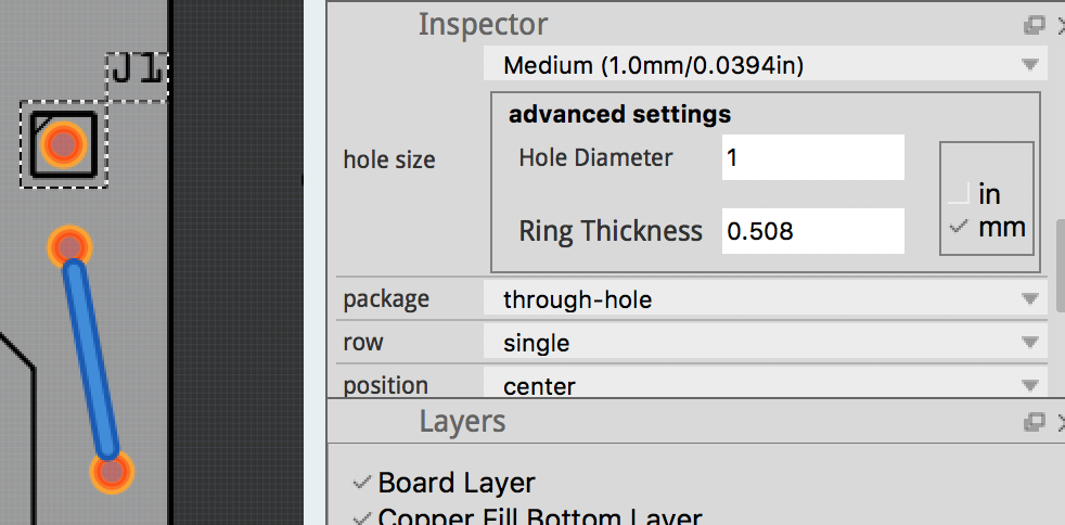
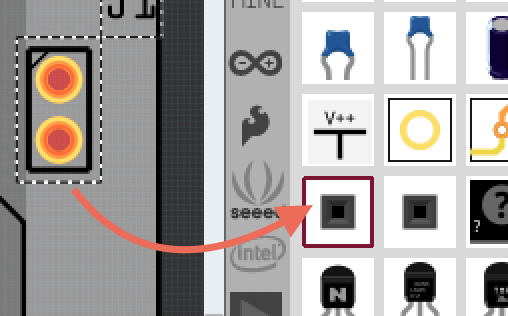
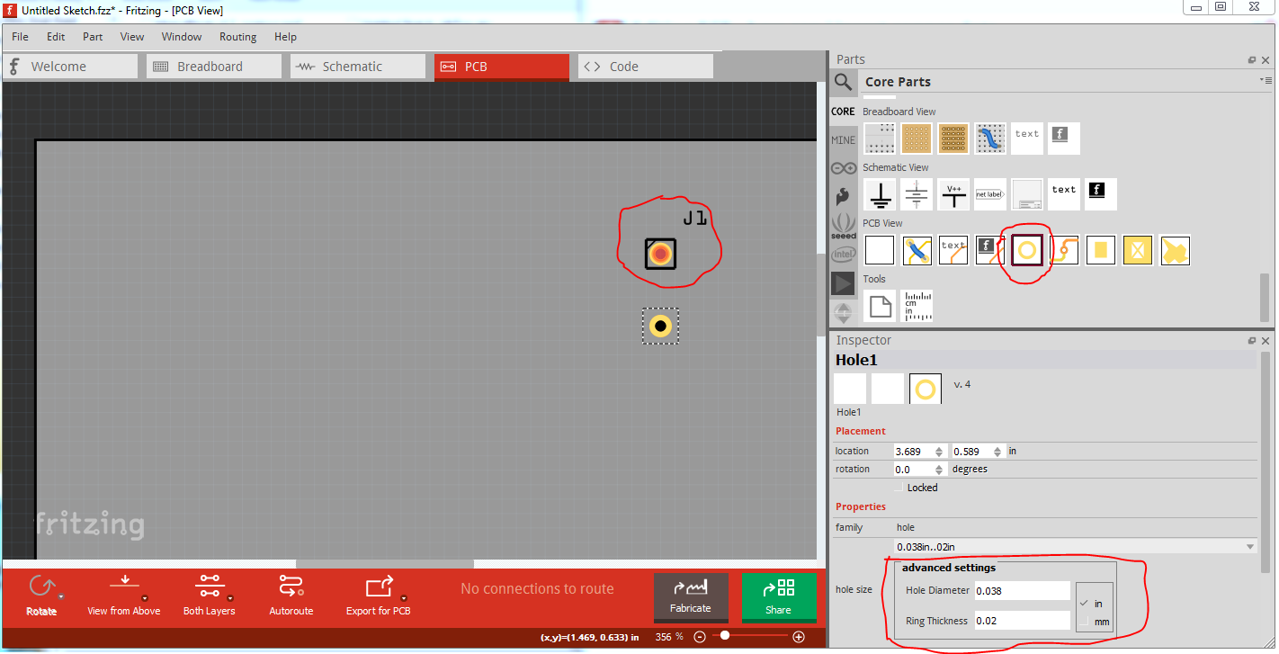
You currently have the top image (a single pin header, which puts a square around it on silkscreen), what you want is the hole below it whose pad has been adjusted in inspector to be the same as a header but which won’t appear at all on silkscreen (so nothing will appear on the print on the top of the board.) To do that you drag a hole (circled in red on the right of the window) from PCB view in core parts, then change the advanced settings in Inspector (bottom right window) to be hole size 0.038in with ring thickness 0.020in (which matches the pad on a .1 header pin.)