Hi folks,
My circuit has grown in complexity and now it makes sense to create a ground fill in order for my components to be routed easily to ground. My question is how to great ground vias.
It seems to me that the best way to create them is to bring in a bunch of arbitrary vias to be board and set them as ground fill seeds. Is this correct? Is there a better way?
There are two ways.
-
as you said already you can place a bunch of vias and set them as ground seeds.
-
create your ground fill and then place the vias (no need to set the seeds)
The advantage of 2 is that it does not create a gap around the vias with traces connecting it. These gaps are required when soldering to a pin connected to the ground fill because the ground fill would pull away the heat too quickly to get a good solder joint. But with vias in the ground fill we do not need this heat break and we would actually rather have it transfer heat really well.
The disadvantage of 2 is that you need to delete the vias and replace them every time you want to re-generate ground fill because if they are in place already it will create the gap. I usually save the file right before placing the vias, generate gerbers and then revert the file back to before the vias were placed.
Ah! #2 makes more sense for my purposes. Thanks!
Can you generate ground fill without automatically generating those randomly placed ground vias?
It will not create any vias on its own. Odds are what you are seeing is vias you have used during routing being blended in to the ground plane.
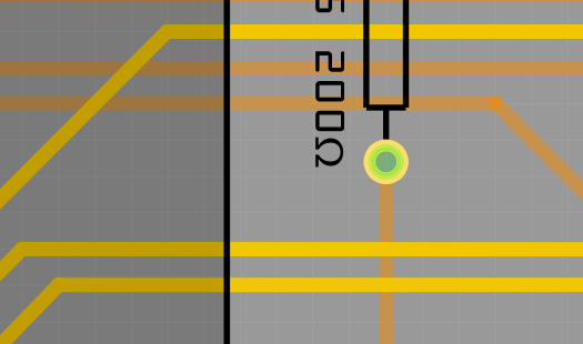
Maybe, but I haven’t added any vias that I’m not using, and I do all the routing manually. See attachments - one with the ground fill shows a via, but when I remove the ground fill it’s gone.
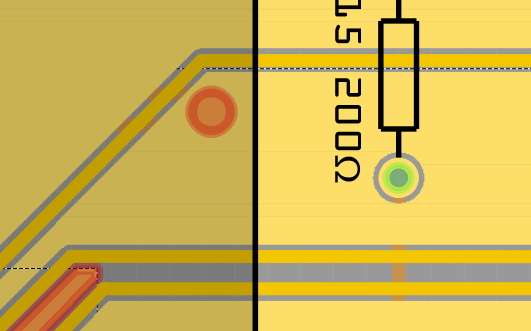
I do not see any vias in that picture. Are you referring to the red dot? That is an unconnected connection point in the ground plane. Fritzing creates those to allow you to connect traces to the ground plane but it is not a hole in the pcb or copper.
Oh OK, yeah that’s what I’m referring to. So I don’t need to worry when I create my ground fill and Fritzing places those directly under existing traces and components on the PCB?
If you are seeing them under a trace it is likely on the opposite side on the solid part of the ground fill. So yo do not need to worry about them at all.
1 Like
You can check the Gerbers to see what is really there, which is something you must do before you send it to fab anyhow. I use the free SW, Gerbv.
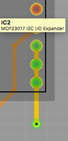
Ok, interesting. I ran ground fill and popped it into the SeeedStudio gerber viewer (this is where I’ll order my boards). Those ground points are gone (great!), but what I’m seeing now is the traces to my ground vias now seem to be just ‘absorbed’ into the ground plane, whereas what I expected was the for just the ground via to be connected to the ground plane, with traces appearing normally just like the rest of the circuit. And it looks like the pins that I’m trying to ground on the components themselves have sort of become their own ground seeds. Here are two images to illustrate what I’m talking about (the red one is from the Seeed gerber viewer). Is this expected/OK?
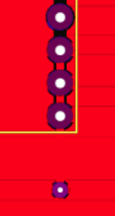
Once you have set a ground seed on any net then everything in that net is part of the ground. If you do not want your actual ground pins to be connected then you would use copper fill. This is what is to be expected and what is wanted since you told it that you wanted that network to be part of the ground plane.
Ok, thanks for all your help!
Ok, so likewise if I choose copper fill and inspect the nets, my ground vias are clearly connected to the copper fill. But what is the fill grounded to? My hunch was that one of the ground pins on my MCU would have been connected to the copper fill, but that appears not to be the case. Maybe I’m overthinking all this, I’m just trying to make sure the board is correct before sending it out.
Copper Fill fills empty spaces but is not connected to anything, unless you connect to one of those red dots, and Ground Fill fill but connects GNDs.
1 Like
As old_grey said copper fill is not attached to anything. Only ground fill connects to the ground fill seed. If you want copper fill but connected you will have to connect it yourself after running copper fill. You can either connect it to one of the red dots like old_grey said or you can drop a via somewhere over the copper fill and connect a trace to it.
1 Like
Thanks, it all makes sense now. So it seems that if I’m choosing to go the Ground Fill way, I don’t even need the additional vias, I can just set ground fill seeds on each component. Is that ideal?
Since all of your grounds should be connected into a single net by traces you should only need to set the seed on a single point and everything that is connected to that net will be part of the ground fill.
The need for extra vias is on a board to board basis. For example you may have an area of fill that does not actuall connect to the ground net because it is surrounded by other nets. In that case you can add a via to connect it to the ground fill on the other side. If the area is small enough you can even delete the small section of ground fill. But this need for them to be all connected depends on what type of circuit you have and how much noise there may be. In most cases unless you are designing high speed communications circuits you do not need to worry to much.
The other reason for adding vias is to move heat from one side of the board to the other. So if you have a voltage regulator or FETs that are dissipating a lot of heat you can add lots of vias to move the heat to the other side of the board. There are many more things that you would want to keep cool those two are just some common examples. If you unsure if a component needs extra cooling check the datasheet for the thermal recommendations.