Are you sure it is not just a rendering issue with Gerbv? Try uploading the sketch via the Fabricate button in fritzing to see how Aisler renders it or try https://gerber-viewer.easyeda.com/ and see if it looks the same.
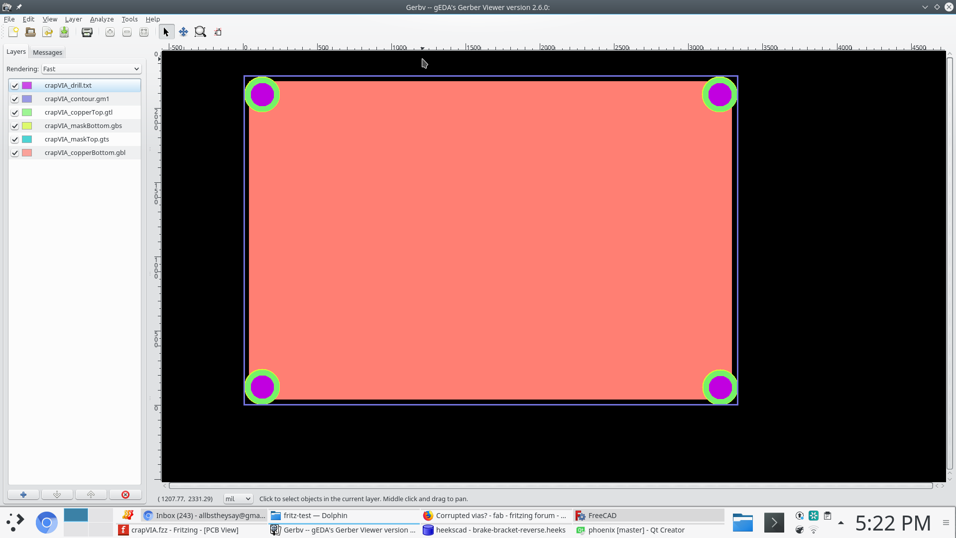
I must ask why you are trying to make over size vias in the corners of a board? There is a mounting hole part that makes holes.
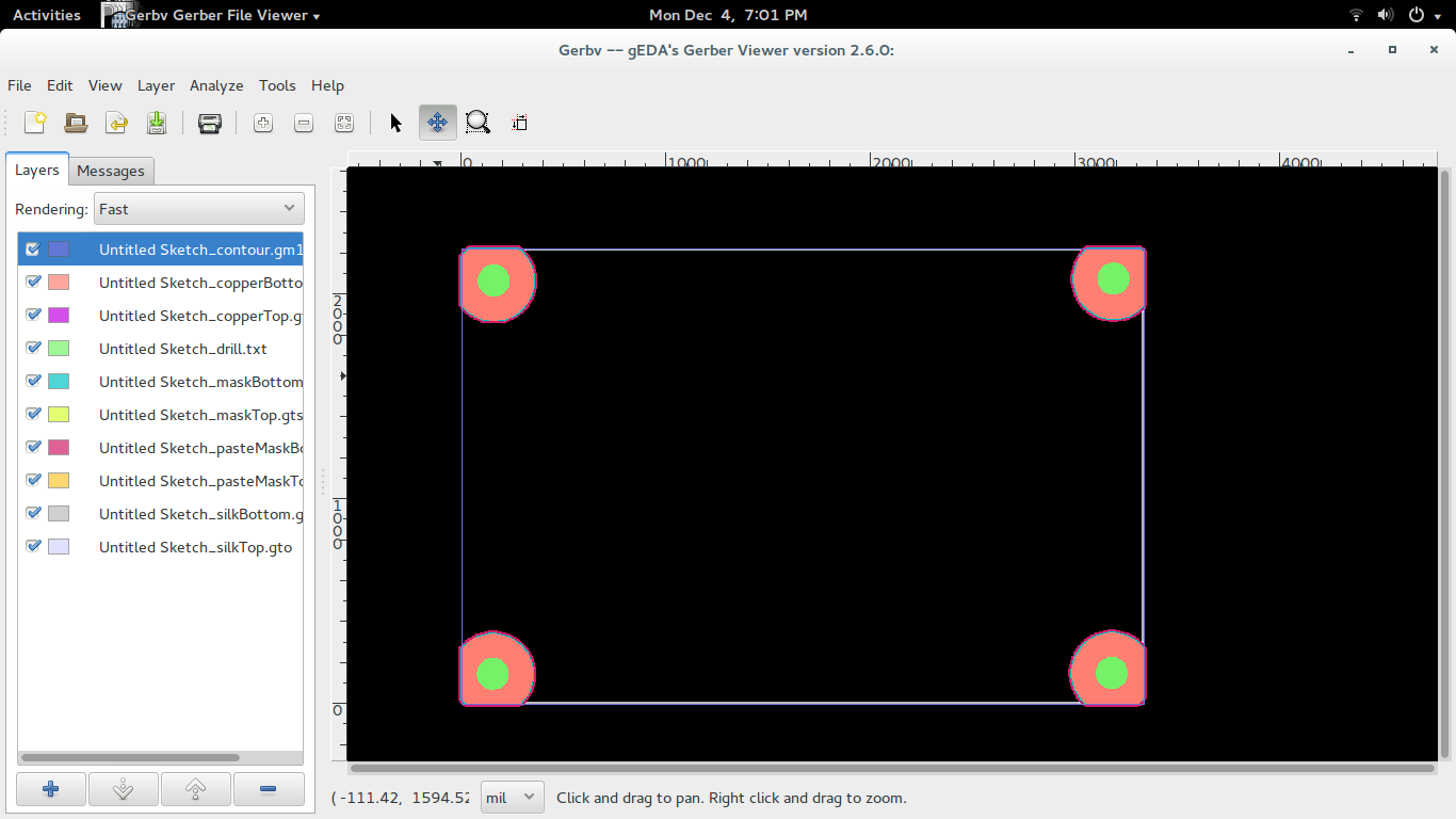
Thanks for the replies! Yes, I have used 4 different Gerber viewers, and multiple projects that show this issue. The purpose of using vias is to have a copper-lined grounding bolt/screw hole, and a mask-free copper area for the screw head and chassis to contact on each side, that a hole would not accomplish. Thanks for confirming the situation OG, and I will simply avoid vias in larger sizes and try to find alternative solutions. Is there a simple way to alter the mask layer to create the contact pads over ground fill around drilled holes?
The Hole part has the same issues. A custom part may be a solution for common sizes (in this case 3.2mm hole and 2mm ring for screw head diameter), but I am not successful in making parts, and it would be a time-consuming effort for a single experiment. Although, it is a last-resort option, so thanks for the idea! I have not tried a header pin or other plated-hole part, as the unmasked ring diameter for contact is not sufficient. Note - the masking seems to be the primary hurdle, if there is a simple way to create the screw head pad by altering the mask. A round copper logo does not seem to punch a hole in the mask.
The size of the ring is adjustable the same way the via diameter is adjustable.
I am wondering if it is the size of the hole or the size of the ring that causes the issue. Can someone try a large ring with a small/no hole and another with a large hole and small/no ring? If either of those work we may be able to figure out a work around to make it work for you.
@Old_Grey could you share your custom part with his dimensions?
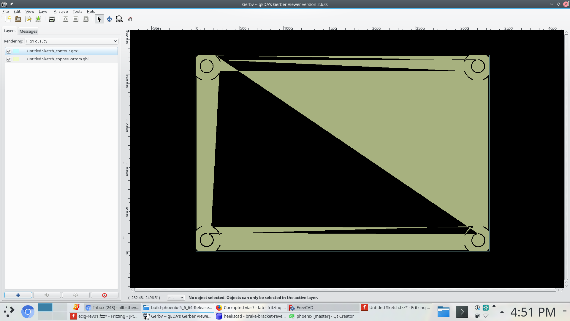
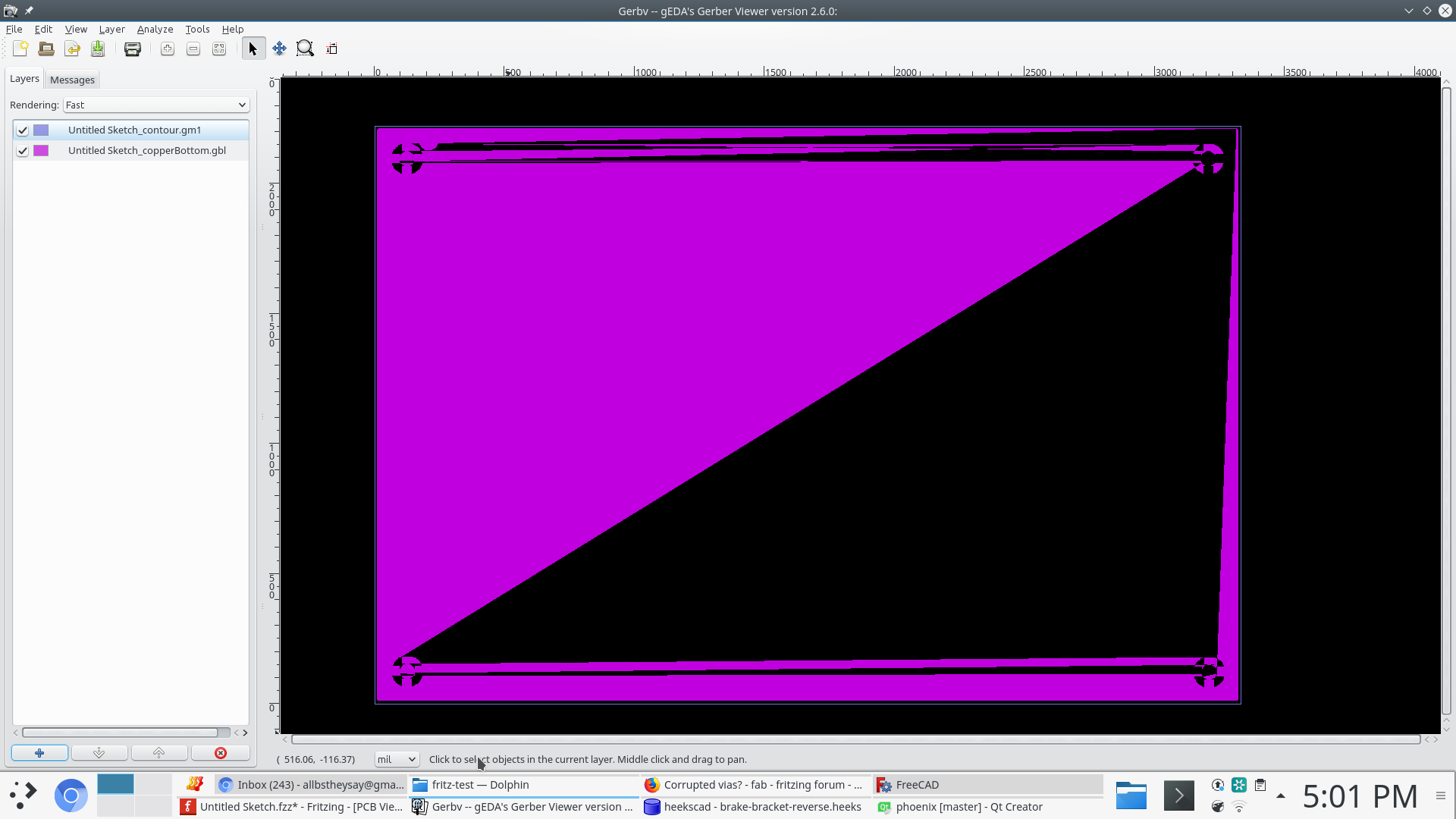
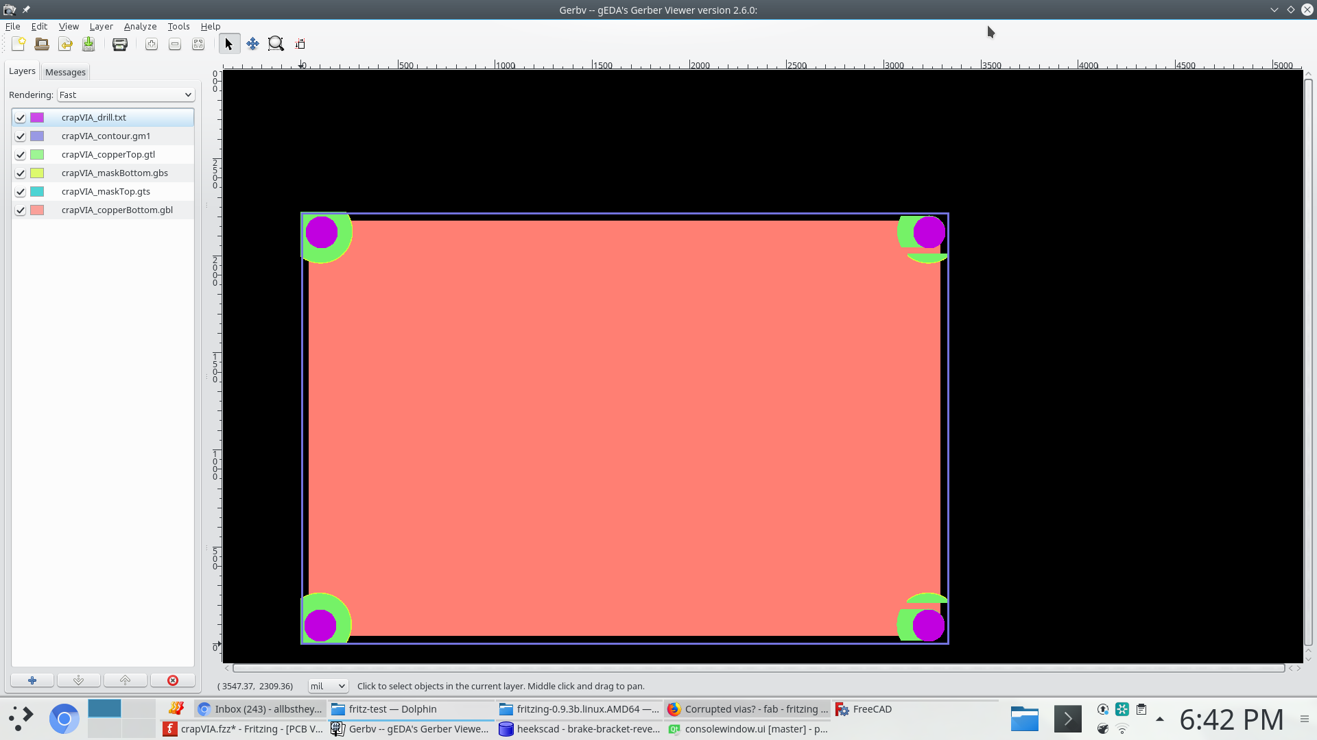
It appears to be a bug in gerber generation truncation on the right hand side (and thus probably not workaroundable). Below is a sketch with a custom part with a 3.2 mm hole and 2mm width. The left is fine in both cases (truncated / not truncated) but truncation on the right is broken (completely within the board works fine as Old_Grey noted). The part should show up in temp as pcb_pad.fzpz. Might be fixed with the new gerber commit if we could get it fixed, but that’s probably the only hope (other than keeping the entire part within pcb or doing the truncation at the svg level in the part). Increasing board size to include the entire pad then moving the board boundary back by editing one of the gerber files may also work, but I don’t know enough about gerber formats to try it.
I do not have enough time to complete this test but maybe @vanepp r @Old_Grey could complete it and test it.
This SVG is a copper path (not a circle so it won’t have a hole) plus a black circle that Fritzing should interpret as a hole. My though is this. I have many parts with solid pads that overhang the edge and I have never seen this even on the right side. I have also placed many holes near the edge again without issue. So this SVG is just that, a pad and a hole. Not a hole with copper around it.
Unfortunatly doesn’t work any better. The bottom right pad is still screwed up. The bottom edge has truncated correctly but the right side has a band cut out of the middle of the copper pad instead of being truncated on the right edge.
Maybe try replacing my copper path with a square? If that works you could try a hexagon or greater sided polygon. When I made the copper path I used a circle and then converted the object to a path but it may have still contained circle information that caused Fritzing to treat it the same as an actual circle.
Replacing the path with a rectangle causes the entire rectangle to be deleted if the right edge is over the right board boundary. Top and bottom truncate correctly, but if an edge is over the right boundary the entire rectangle isn’t in the gerber. But when the going gets tough the tough get twisted . This is extremely ugly but seems to work. I changed back to a circle and then offset the drill hole (as it is independent). It renders on pcb in fritzing wrong (the hole isn’t offset) but the gerber is correct (although you need to rotate the top copy by 90 degrees to get the hole correct and you can’t see it except on the gerber.) I expect it would be better to replace the circle with a square to get more copper area for the screw head to contact but this should do what he wants in an ugly way.
I do believe a square with an offset hole would be the easiest solution but I do have another that should in theory work well but will end up being harder to use.
Create a single SMD circle part. You would have to place a copy on both sides and then place a hole over the part. I realized all the parts I overhang on my boards are SMD parts because they are edge connectors and mounting pads. Even if it does still have the problem you could export the gerber files and then delete the holes and re-export the gerbers to a new location. Then you could use the drill file from the first export with the other layers from the second export which again should solve the problem because the missing portion looks to always involve the hole.
Thanks for all the efforts everyone! In the interim I have tried several other workarounds, none of which was functional, except for an off-center no-overhang Pad with a small-ring via similar to Peter’s solution and Sub’s suggestion. While not quite what I’m after for a clean circular screw-head pad, and somewhat limiting, it will do for now to get the job done. If anyone has ideas for easily modifying the masks in order to expose ground fill, it may be a simpler go-to solution for similar stuff in the future?
Well I’m not sure what you guy’s have been up to… Maybe, it needs a particular order of operation…? Not sure, BUT, if this was me, looks like it works just fine. I’ve included a few files. Maybe you guys can see whatever you are doing wrong.
Might have something to do with saved files. Because my first test was laughable. Not sure there is a bug, or what exactly that is all about. But something fishy does exist. I think within a file labeled untitled.
So that worked… So I decided to fudged a bit more. If I was using this PCB to ground to a chassis, this is exactly how I would run it. Place VIA’s exactly as you would want them. Then all 4 resized to small .4mm holes, then bottom only copper ground fill. After fill, resizing VIA’s to 4mm/.9mm ring. Beauty
@landracer none of your holes were overhanging as far as the OP’s were. They had a very large portion of the pad overhanging the edge of the board which causes this issue.
Your file (because it is all within the board boundaries) works fine. However the OP has the center of the mounting holes near the edge of the board so the pad extends over the boundary of the board so the pads should be truncated and that breaks (as does yours when I reduced the width of the pcb to 82cm) but only in the gerber output in gerbv, fritizing still looks fine.
It’s an easy fix by making the grid size smaller and moving the vias in, but the fact is this will probably never be fixed because people smart enough to fix it will never use FZ because it looks too beginner and below them.
 . This is extremely ugly but seems to work. I changed back to a circle and then offset the drill hole (as it is independent). It renders on pcb in fritzing wrong (the hole isn’t offset) but the gerber is correct (although you need to rotate the top copy by 90 degrees to get the hole correct and you can’t see it except on the gerber.) I expect it would be better to replace the circle with a square to get more copper area for the screw head to contact but this should do what he wants in an ugly way.


 Well as they say… IT must get worse, before it gets better!