I am trying to make 2 custom parts, a Relay and a PSU
I have a BB image, a Schematic and a PCB, they all load into parts editor, but when i save the part and try and load it, i just get a big coloured square that doesn’t really do anything in the breadboard and PCB views…
Here is a link for the SVG files for my 2 parts, they all load ok into fritzting part editor but when i save that and drag them in its just a colour block…
Thanks for any indication as to whats wrong with these files, ive spent forever on them and im sure im overlooking something
I can’t do much without the .fzz or .fzpz files, but by the sounds of it there is a big red box over the part. This tells you the pins haven’t been assigned.
how do i get those files? I can provide them if needed, im not assigning pins as im a graphic designer not the technical guy, i just need the part imagery working or to test if its correct, i have zero knowledge on the pins part!
The fzpz would come from the part that you are trying to load the svgs in to, however I can tell you your problem from looking at the svg files you posted which is unfortunatly that you don’t have any connectors (and the fzpz from the part you are basing this on does and thus you get the red screen indicating missing connections). For the relay you would probably be better starting with one of the existing relays and changing it (and its connections) to match the one you want. For the power supply, you look to be using the daughter board with screw terminals as the connectors and would thus probably be best to copy/paste (and then edit in the connections) an appropriate screw terminal connector from core in to your current svg. Bottom line is you likely can’t do this ignoring the connectors, Frtizting won’t work that way. You may be able to edit out the connections in the base fpz file you are using to get it to load only the images (I’ve never done that so I don’t know if it will work).
There isn’t really anything that I see that is that close, here are a couple of choices that may help:
relays:
the rt424f05 latching relay is probably your best bet.
power supply
this is similar but without the screw terminals
For screw terminals search in fritzing parts bin for screw terminals
the camdenboss ctb0158-2 seems close to what you want but you need to know the pin spacing of that ever is on the board you are using. I don’t think any of these are surface mount though.
Inkscape won’t open the svgs in your latest zip for me. It would be easiest if you export the part directly from frittzing (assuming you are now getting a part in Fritzing of course). To do that right click on your part in the mine parts bin and select export part. That will create a fzpz file with the fpz file and all of the svg files for the part. You can then upload that file here via the 7th from the left icon in the tool bar at the top of the reply box here in the forum. The gold circles are because the relay I referenced is through hole rather than surface mount so you probably want to keep your original pcb svg and just add the connectors from a surface mount part (this is what I meant about the parts not being quite the same). As to the psu, yes you can make only one part but you are going to need to use cut and paste in (in my case Inkscape, I assume the other packages have a similar feature) to copy parts of the screw terminals in to the svg. You will need to edit the xml and probably the fpz file as well to make the connections work. If you can get to the point where you can upload a fzpz file one of us will probably be able to help you do that as it isn’t simple (not much about parts creation is simple unfortunatly, that’s the price we pay for Fritzings unique features).
When i create my part i generally drag a random part in and just add my images to each of the tabs, will this cause issues? is there a way to create a part from fresh and not edit an existing one in editor? As i say im not the technical guy so i dont know about connectors and stuff, im just trying to get working images sorted for the technical guys
That is generally the recommended way to make new parts. It is possible if you are familiar enough with parts editing to make one from scratch but you generally (or at least I do ) need to run it through parts editor to get it properly registered with Fritzting afterwards anyway. If you upload the fzpz file after you have added your images (even if it shows as a red screen in fritzing) one of us can probably wrangle the connectors in such a way that you can see your images in fritzing to do what you need, the connectors being incorrect are what is blocking frtizing from showing your new images. With all of the files I can (and usually do) use a text editor for the fpz file and Inkscape for the svgs to get it to a state that Fritzing will load.
Ok i gave it a go by adding my images to the Relay you posted previously, i do hope this is of use as im really struggling to get my head around the technical aspects of this software vs the images! The reason for the messed up text is fritzing bugs out when i try and load in OCRA or Droid Sans fonts from illustrator so i have to outline them and then it decides to render them oddly as you can see, so many issues!
and they may work better than the ones you have (I use Windows were they work fine, you look to be on a Mac). I’ll have a poke at your part and see what I can fix up.
yep im using those fonts, but if i save in illustrator and try and load the svg in fritzing it says im using fonts that aren’t allowed, even though im 100% using the ones in your link
Maybe one of our illustrator users will have a comment on how to do it, I use Inkscape (mostly because its open source) and it just works at least mostly there, although fonts are sometimes a problem.
yeah i tried inkscape and also tried windows and im always having issues, this work around should do the job for now, it just doesnt look perfect. Any feedback on that part?
Here is a better (but still not perfect) part. I replaced schematic svg with the original from my relay and modified it to match what you appear to want (only the no terminals and common). I added terminal rectangles to the bb svg (the groups won’t serve as terminals it needs an entity on the board. In pcb I moved the silkscreen so it wasn’t overlapping the copper (I don’t think it is correct, but I don’t normally make sm parts, perhaps one of the other folks that do will comment). In all three svgs and the fpz file I corrected the pin numbering to match the svgs. Last but not least I removed all the pxs that Inkscape sprinkles through the svg files as they break Fritzing eventually (after editing the part a time or 2 the font size gets reset to 0). Replaced the path text with standard fonts in bb and schematic on the way by. I’ll have a poke at the power supply board for a bit and see what I can do there as well.
(edit: and the ps module built from a generic 4 pin IC base with your breadboard image copied in a slightly modified generic schematic and your pcb with connectors corrected to match the fpz file. )
Thanks sorry for the delay i assume we are in different time zones, i tried the relay, it seems to not fully sit on the BB or is it meant to look like this? I assume its because the 10 connectors havent been added to the part? Also when i try and export SVG files from the part, the BB image is just a black rectangle and has no text or styling to it, any idea?
Also it seems to make sense i post you the technical drawing for the part rather than assumptions, here is the relay data, using the non-latch type, the schem in the part looks way off, its missing pins 2 and 9, and its layout inside doesnt match. On the PCB 4 of the pins arent clickable either I assumem again its because the 10 connectors havent been added to the part?
on breadboard note the connectors are connecting to the middle of the pin, typically they should connect to the end of the pin (which is achieved by moving the terminal rectangle in the svg to the end of the pin). Usually the pins would be on .1 centers but in this case the horizontal spacing is .38 inch, so it won’t fit on a standard breadboard and thus yours looks correct and we just live with it (its usually best if parts match the real world). In schematic same problem same solution: move the terminal rectangle to the end of the pin and the connection (at an angle) will pivot on the end of the pin as it should (if you do this same thing with the part I posted last night you will see what I mean, there the connector bends at the end of the pin as it should). With the note that I rarely use PCB and surface mount even less so my advise may be suspect (hopefully one of the pcb experts will chip in here!) the silkscreen is overlapping the copper of the pad and I think that will be a disaster when you attempt to solder this. As noted I don’t know what the standard thing is for a silk outline on a surface mount component but I’m pretty sure this isn’t it . Again the pad is defaulting to the center of the pad area which may or may not be how it is supposed to work, again I don’t know what is standard here. You can get the proper alignment if you manually route the traces correctly so perhaps this is how it is usually done.
thanks so the part i posted is atleast usable if not perfect.
In regard to the PCB it over laps as the part on the inside of the silkscreen would be under the chip and fold round and outward as per the technical specs, so obviously there has to be overlap from the pin legs as in the real world they would be under the chip and protrude out from the sides? Or is that now how the PCB should work for this part
Yep it looks to work fine the issues are cosmetic. As noted I’m not experienced in surface mount , but a silk screen layer over the connection area is I think likely to cause a soldering problem (a I think the silk screen is later in the pc production process). Hopefully someone knowledgable in surface mount (which isn’t me will comment.
 ) need to run it through parts editor to get it properly registered with Fritzting afterwards anyway. If you upload the fzpz file after you have added your images (even if it shows as a red screen in fritzing) one of us can probably wrangle the connectors in such a way that you can see your images in fritzing to do what you need, the connectors being incorrect are what is blocking frtizing from showing your new images. With all of the files I can (and usually do) use a text editor for the fpz file and Inkscape for the svgs to get it to a state that Fritzing will load.
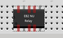

 . Again the pad is defaulting to the center of the pad area which may or may not be how it is supposed to work, again I don’t know what is standard here. You can get the proper alignment if you manually route the traces correctly so perhaps this is how it is usually done.