Hello, this was my new attempt on making custom
I followed the video below:
and my work:
2019simpstaOCT.fzz (67.8 KB)
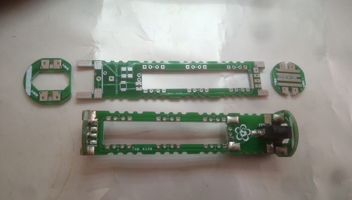
you can see the board is designed to cooperate with other 2 boards, and can assemble to a 3D product.
The boards were all 1.6mm in thickness and the slot for assemble is 1.7mm tall and 3.2mm wide, for a 1.6mm*3mm latch to insert, there’s still little margin to move but not much.
I followed the video to create board shape,
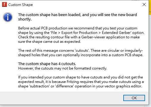
but with complicated shapes there will be errors,
the errors won’t show up when importing svg to fritzing but after exporting to gerbers,
from gerber viewer the shape was randomly wrong and unusable.
notice the CUTOUT numbers, its the numbers of PCB shapes going to yield after your PCB made (includes working PCB and the windows cutting out, for this SVG there’s 4)
If the numbers correct its usually right
I found out, after completing editing shape and naming the layers “board,silkscreen” and the “boardoutline” path.
Then the last thing you do was to do the intersection it with a bigger square, to force the product a good path and don’t edit after.
silkscreen layer was not always needed, but helpful to point out the edge where your real silkscreen’s limit were.
also I’ve found that by placing vias close enough to the edge inside, you can make “Castellated Holes” , useful in some kind of sinking- though hole device, or creative use.
 .
.