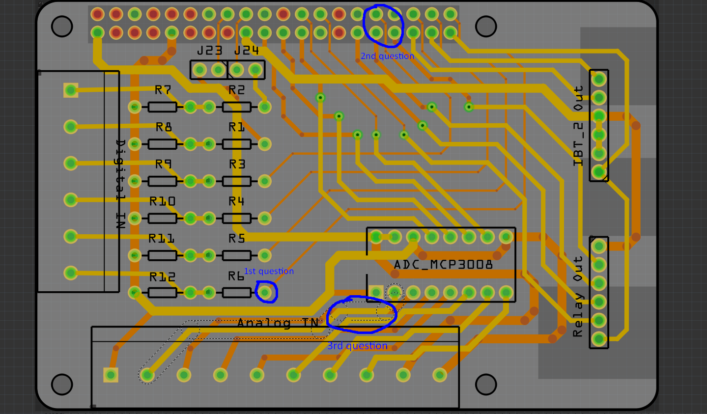
1st question:
How can I make the holes of the resistors smaller?
They seem to be on the default 1mm, but I need them around 0.7-0.6. There is no option when I click on them.
2nd question:
How can I make a wire partly smaller, and then bigger again?
On the 40pin connector, some wires need to be small, in order to fit-pass between the second line of connectors.After that, I want them to be bigger again, cause I am afraid of voltage drop on a constantly slim wire.
In the picture below, I need the section of wire in the blue circle as it is, and the rest of the wire bigger.
3rd question:
Is there a problem with close to another wires?
In the picture below, the dotted line from one wire, intersects with another wire. Am I going to have a problem with them being too close to eachother?
1 - You have to go into the part and modify it’s svg drawing and make it a custom part.
2 - You cut the trace by right-click deleting a section up to a bend point, size both parts in the Inspector, and then joining them back up again.
3 - The closeness of traces depends on how accurate it’s going to be etched. Production houses can get them close, home etching depends on how good you are.
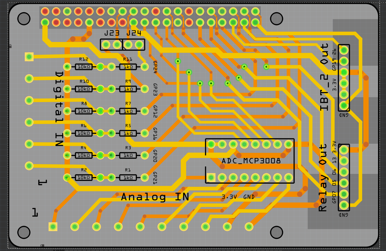
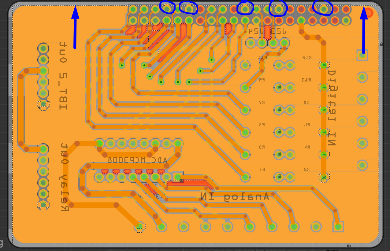
Just a final question, I need to fill the bottom with Ground, but it seems to be prefixed on the perimeter.
As a result, it doesn’t catch up with the 5 outter GND Gpio’s from RPi.
Is there any way to make it hapen?
Yes, the underside I mean, but I know how to fill it.
The problem is with the 5 GND pins, in the blue circles, which are not included in Ground fill, bacause it has a limited perimeter. I need to extend the Ground fill, tothe blue arrows direction, in order to include these 5 pins.
How can I do it?
It would be a good bet to export the gerbers (file->export->for production->extended gerber) and the check them with a gerber viewer (I use gerbv from the geda project but there are others) to make sure the board looks ok in the gerbers (as that is what the production house will make if you aren’t doing your own)